Start with what you need delivered: a bare board, a stencil or an assembled prototype.
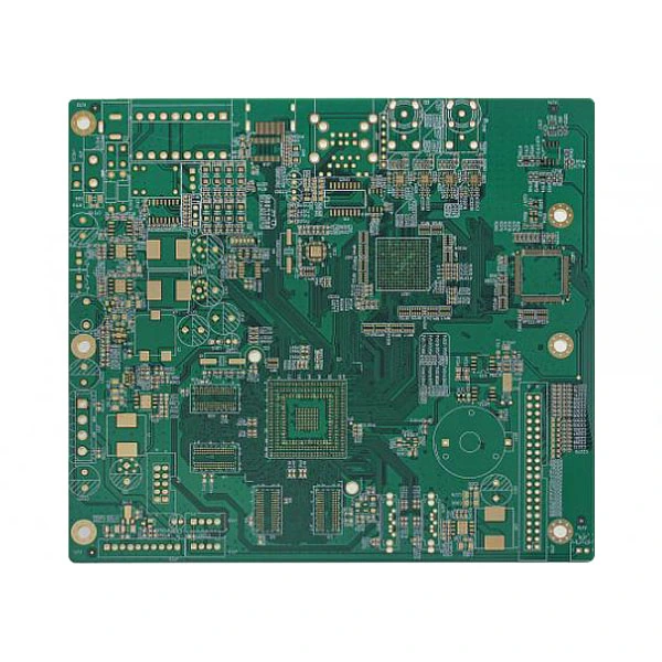
深圳市德群快捷电子有限公司 · Dequn Quick PCB describes a Shenzhen-based quick-board operation established in August 2013, with FR-4 fabrication, laser-stencil services and SMT assembly. Its published design rules accept 1–10 electrical copper layers. The catalogue gives more specific examples: double-sided boards, four- and eight-layer boards, a six-layer half-hole board and a BGA board.
01 / BARE PCB
Release the fabrication drawing.
Gerbers, drill definitions, netlist, stack, copper, solder mask and profile. Identify which hole dimensions are finished values and which are drill-tool sizes.
The distinctions matter for a “quick-turn” enquiry: a fabrication lead time is not automatically the delivery time of a populated, tested board. Ask for separate engineering-release, material-availability and shipment milestones.
CORRESPONDING ORIGINAL CATALOGUE IMAGES
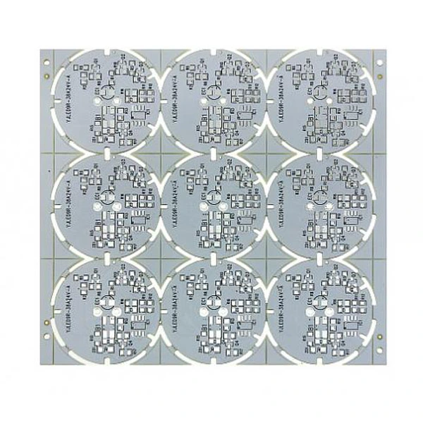
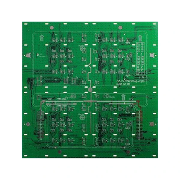
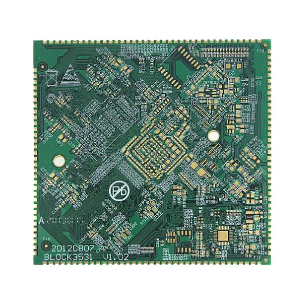
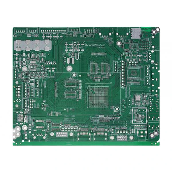
Five constructions to compare before sending files.
The official product page repeats a 4 mil line / 4 mil space entry and a 0.3 mm “via” entry alongside these examples. Those are manufacturer-published entries; they are not measured results from the pictured boards. The via wording does not define a finished plated hole.
Double-sided white-mask PCB
Electrical layers
2, from the double-sided title
Mask title
White solder mask
Published line / space
4 / 4 mil
Via entry
0.3 mm; finished-hole definition not provided
Specify the mask ink, finished dimensions and finished plated holes on the fabrication drawing. Confirm whether the quoted geometry and mask openings can be delivered together.
Four-layer green-mask PCB
Electrical layers
4
Mask title
Green solder mask
Published line / space
4 / 4 mil
Via entry
0.3 mm; finished-hole definition not provided
Approve the stack and inner/outer copper before quoting. The green-mask title conflicts with the repeated white-ink paragraph; release the actual mask colour and ink requirement.
Six-layer half-hole PCB
Electrical layers
6
Construction title
Half-hole board
Published line / space
4 / 4 mil
Separate half-hole rule
Minimum 0.6 mm
Send the edge-plating and routed profile drawing. Ask for the finished castellation diameter, annular land, breakout and burr acceptance; the generic 0.3 mm via entry is not a half-hole limit.
BGA board example
Catalogue title
BGA board
Layer count
Not specified for this example
Published line / space
4 / 4 mil
Via entry
0.3 mm; no BGA-pitch acceptance stated
Release the package footprint, mask openings and assembly requirement. Confirm whether mask bridges are needed: the general service rule says they are not offered in the stated fabrication service.
Eight-layer PCB
Electrical layers
8
Published line / space
4 / 4 mil
Via entry
0.3 mm; finished-hole definition not provided
Stack and impedance
No sample-specific stack or tolerance supplied
Define the eight-layer stack, reference planes, finished copper and panel routing. Any impedance target needs an agreed tolerance, coupon and measurement plan instead of inheriting a general process limit.
FABRICATION INPUT / TWO VERSIONS OF THE SAME OFFICIAL RULES
A cutting panel is not the maximum size of your design.
WORKING PANEL1200 × 510 mm
The official explanation identifies this as the material cutting / working-panel size.
CUSTOMER DESIGNUsually within 380 × 380 mm
This is the separate customer-design guidance on the same page, subject to file review.
Send finished dimensions, panel rails, routing slots, breakaway method and quantity together. Do not quote a 1200 mm finished board from the working-panel headline.
Stack and copper
Electrical layers
1–10
Accepted material
FR-4; specific brand, grade and Tg not supplied
Board thickness
0.3–3.0 mm; stated available discrete thicknesses should be confirmed for the chosen stack
Thickness tolerance
≥1.0 mm: ±10%; below 1.0 mm: ±0.1 mm
Finished outer copper
1–2 oz; 1 oz described as the default, 2 oz needs an order note
Finished inner copper
0.5 oz in the published rules
Confirm the dielectric stack and copper distribution for a multilayer design. These separate rows do not establish that every layer, thickness and copper value can be combined.
Geometry and holes
Minimum trace / space
4 / 4 mil; the rules recommend larger geometry where possible
Mechanical drill tools
0.25–6.3 mm, in 0.05 mm steps
Half-hole minimum
0.6 mm
Profile tolerance
±0.15 mm
Trace to routed edge
At least 0.3 mm
Trace to V-score centre
At least 0.4 mm
The hole-tolerance row is headed mechanical drilling (±0.08 mm), but its explanation uses a finished-hole example. Ask for explicit drill-tool, plated finished-hole and non-plated-hole tolerances; the directory does not resolve that ambiguity by assigning a finished-hole minimum.
0.1 mm; the rule says solder-mask bridges are not offered in that stated service
Routed panel gap
At least 2.0 mm for the gapped-panel route
Legend
Minimum 6 mil character stroke and ≥1 mm height
Outline input
One authoritative outline layer, not two competing profiles
The fabrication rule distinguishes the solder-mask layer from the paste layer. That does not mean the paste layer can be omitted from a separate stencil or assembly order. Identify the deliverable before applying a bare-board instruction.
BARE BOARD → PASTE PRINT → PLACEMENT → ACCEPTANCE
Keep each acceptance step attached to its own deliverable.
Laser-cut stencil
The manufacturer says it established the SMT laser-stencil division in 2018 and can modify aperture data. Agree foil thickness, frame, fiducials, paste type and aperture drawing revision. Its advertised 1 μm repositioning statement is not a supplied acceptance report for a finished aperture.
Placement and soldering
The SMT section describes three Panasonic placement lines, BGA/QFN handling, automatic and semi-automatic paste printing, a Jintuo N-800 eight-zone lead-free reflow oven, and wave/DIP work. It lists 0402 and 0201 without defining the package-code system. Specify the actual dimensions and manufacturer part numbers rather than assuming a size convention.
Inspection and functional result
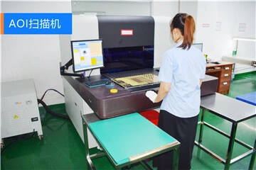
The same section names AOI and solder-paste thickness measurement. Those inspection methods do not by themselves establish functional testing. Ask for the actual inspection coverage, any X-ray/ICT requirement and the power-up or functional-test procedure included in the quote.
A short RFQ package for this service
Revision: one fabrication release, controlled paste files, placements and matching BOM.
Material: FR-4 grade, stack, copper, finish, board dimensions and any approved substitution policy.
Components: approved part numbers, sourcing responsibility, customer-supplied parts and shortages.
Schedule: engineering approval, laminate/components availability, assembly slot and shipment date as separate milestones.
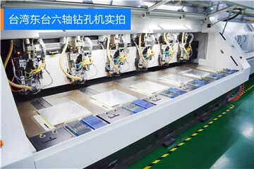
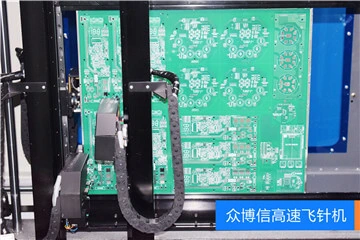
Manufacturer-labelled six-axis drilling machineSeparate tool size, finished hole and plated-hole tolerance.AOI scanning stationAsk which bare-board defects are covered and which reports are supplied.Manufacturer-labelled flying-probe equipmentAgree netlist-linked continuity and isolation acceptance, separately from assembly functional testing.
The equipment page’s Shenzhen description dates its procurement list to June 2016: drilling, PTH, plating, exposure, profiling and flying-probe equipment. Its quantities are historical manufacturer statements, not a current inventory or reserved capacity for a new order.
ENTITY AND LOCATION / CONFIRM THE ROUTE ON THE QUOTATION
The order needs a named producing site, not only “Shenzhen”.
Longgang, Shenzhen
The contact page identifies the Shenzhen plant at Building 3, No. 48 Pingzi Road, Nianfeng Community, Pingdi, Longgang. The equipment introduction describes the headquarters and a nearly 5,000 m² quick-board base without a current dated capacity statement.
Shajing, Shenzhen
The contact page calls this the Shajing marketing department, at the first floor of Building 3, Haosi Western Industrial Park, Heyi Community. The equipment navigation instead says “Shajing factory”. Confirm whether your fabrication or assembly is actually performed there.
Lipu, Guilin
The contact page names a Guilin factory at Building 13, Jinjiping Industrial Park, Xinping, Lipu, Guangxi. The read pages do not establish the legal contracting entity or assign each pictured product to this plant. Request that allocation on the quotation.
A dated government record identifies the Shenzhen entity.
The Shenzhen Science, Technology and Innovation Commission’s original 2023 first-batch proposed high-tech-enterprise cultivation subsidy list names 深圳市德群快捷电子有限公司 at row 6467, PDF page 127. The list is a proposed-subsidy record. It is not evidence that the payment occurred, a current certification check, or an approval of the PCB/SMT processes described above.
The official contact page publishes sc@dqkjpcb.com and telephone +86 755 89311909. They were checked against the website; no mailbox-control test or outbound message was performed. Keep the buyer enquiry in PCBVerified and ask for the named entity, producing address and agreed inspection documents.
SOURCE TRAIL
Sources behind this profile
Individually researched 9 October 2026 from the complete official pages, corresponding original catalogue photographs and the original government PDF. The repeated mask-colour paragraph and hole-definition ambiguity are retained as questions, not silently resolved. No numerical limits were inferred from images and no quality or certificate badges were assigned.