

MANUFACTURER DOSSIER
Delton Technology (Guangzhou) Inc.
广州广合科技股份有限公司 · Guangzhou, Guangdong, China
Company facts at a glance
- Chinese legal name
- 广州广合科技股份有限公司 (traditional: 廣州廣合科技股份有限公司)
- English name
- Delton Technology (Guangzhou) Inc.
- Short names
- 广合科技 · Delton
- Listings
- Shenzhen Stock Exchange Main Board, A-share 001389, listed 2 April 2024; Hong Kong Stock Exchange Main Board, H-share 01989, listed 20 March 2026
- Founded
- 2002
- Registered address
- No. 22 Baoying South Road, Guangzhou Free Trade Zone; the website also lists No. 18 Baoying Avenue
- Production bases
- Guangzhou; Huangshi, Hubei (subsidiary); Dongguan drilling and machining (subsidiary); Prachinburi, Thailand, in production since June 2025
- Capacity, Jan–Sep 2025
- Design capacity and actual output from the H-share prospectus: Guangzhou 780,000 m² / 770,000 m²; Huangshi 724,000 m² / 552,000 m²; Thailand 150,000 m² / 18,000 m². Full-year 2025 area figures are not published.
- Process capability
- No company-wide limit table. Product pages give typical values such as 20 or more layers, 0.075/0.090 mm line and space, 0.2 mm drill and 15:1 aspect ratio; the 2025 report describes UBB boards of 28 to 46 layers.
- Certificates on the website
- ISO 9001, IATF 16949, ISO 13485, ISO 14001, ISO 45001, QC 080000, ISO 27001 and an ISO/IEC 17025 laboratory accreditation, among others, listed with certificate numbers per site but without dates
- UL files
- E237771 and E198991, printed wiring boards (ZPMV2), and E532296, flexible constructions (ZPXK2), all held by Delton Technology (Guangzhou) Inc.; E494566 belongs to Delton Technology Ltd, Hong Kong
Checked on 29 October 2026 against the 2025 annual report on CNInfo, the 2026 H-share prospectus on HKEXnews, the official website and UL iQ for Printed Wiring Boards. Ask which base will build your stack before comparing quotations.
Start with the channel and connector requirements.
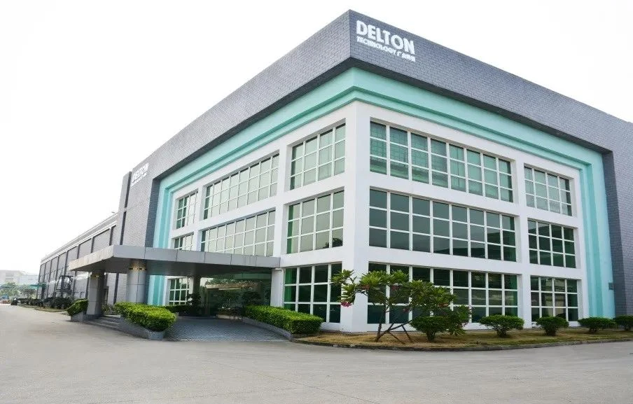
Delton Technology (Guangzhou) Inc. (广州广合科技股份有限公司) was established in Guangzhou in 2002. Its current catalogue concentrates on high-speed and high-frequency PCBs for data centres, servers, AI platforms and communications, alongside industrial, automotive and other applications. This profile examines four separate fabrication examples; it is not a catalogue of assembled servers.
The Guangzhou contact page gives No. 22 Baoying South Road and No. 18 Baoying Avenue. Put the contracting company, actual fabrication address and any drilling subcontractor on the quotation. A group-level capability is not automatically a capability of every site.
The original 2025 annual report confirms the legal identity and Guangzhou registered address. It distinguishes Huangshi PCB production, Dongguan drilling support and a Thai fabrication subsidiary; Thailand began production in June 2025. Ask which qualified site will build the quoted stack and who approves a transfer.
Catalogue dates and newer disclosures
The server and switch pages are dated December 2022; storage and UBB pages are dated May 2024. Keep their stated constructions intact. The 2025 report separately records PCIe 6.0 transfer-to-batch capability and 400G/800G switch-board volume production. These dated disclosures do not upgrade the pictured PCIe 5.0 board or supply a guaranteed loss limit for your channel.
Translate “16 GHz monitoring” into an agreed test.
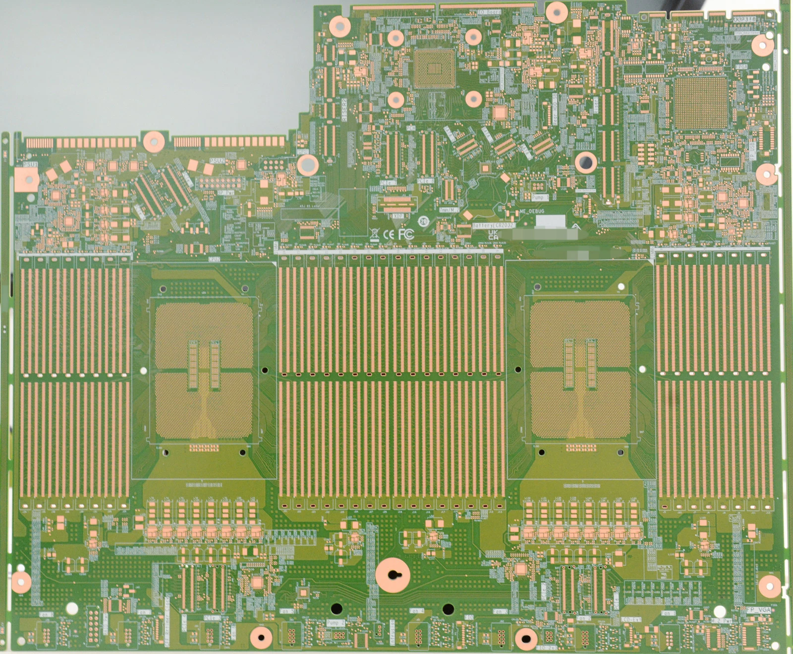
- Named platforms
- Intel Eagle Stream / AMD Genoa
- Design layers
- 14 or more
- Published hole wording
- 0.2 mm minimum aperture
- Back-drill design
- D + 8 mil
- Insertion-loss monitoring
- Up to 16 GHz
- Laminate description
- High-speed material; grade unspecified
The hole wording does not identify a finished plated-hole acceptance. D + 8 mil is a back-drill callout, not a residual-stub length. Return a hole map with through-drill diameter, back-drill diameter, entry face, stop layer and remaining stub separately defined.
The page discusses pulse VCP plating, plasma desmear, LDI, vacuum etching, high-speed solder mask and low-profile brown treatment. These describe process needs; they are not a current equipment inventory. Ask for the assigned line, plating criteria and construction-specific qualification evidence.
Specify the insertion-loss limit versus frequency, coupon geometry, reference planes, de-embedding method and delivered test record. A monitoring frequency alone says neither how much loss is acceptable nor whether a connector-plus-board channel passes.
Specify which layers need the low-loss material.
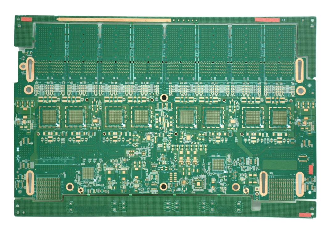
- Typical design
- 12 layers or more
- Trace / space
- 0.075 / 0.090 mm
- Machining aperture
- 0.225 mm
- Thickness / hole ratio
- Above 9:1
- Material strategy
- Ultra-low-loss / ordinary FR-4 hybrid
- Discussed processes
- Back drilling, resin fill and POFV
The catalogue describes hybrid lamination to reduce cost. Its material classes do not identify a CCL or prepreg grade. Provide a layer-by-layer dielectric schedule, approved grade, resin content, glass style, finished copper and foil profile. Ask whether any proposed substitution changes the loss model, lamination cycle or registration.
For optical-module and high-speed connector regions, distinguish filled/capped pads from press-fit and back-drilled holes. Include via-fill material, copper cap and planarisation acceptance where relevant. The 0.225 mm value belongs to machining language and is not silently labelled a finished plated-hole diameter.
This example’s finer trace/space values do not inherit the server page’s 16 GHz measurement or its D + 8 mil callout. Agree the switch stack’s loss budget and back-drill release independently.
Freeze the mating and press-fit definitions before drilling.
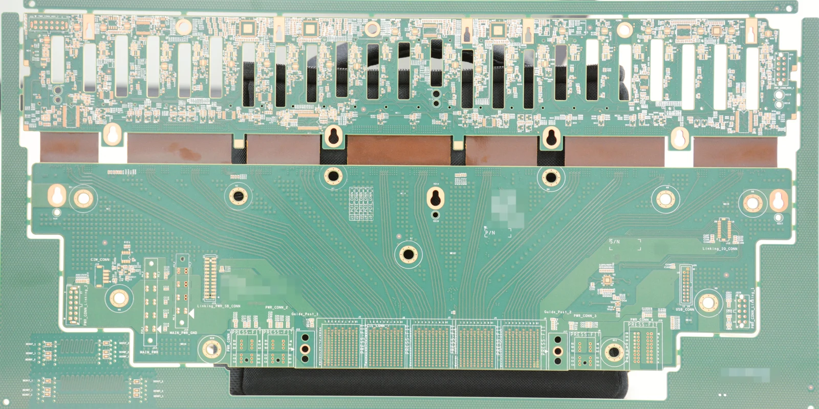
The storage page describes a thick multilayer backplane with multiple drive connection ports and high-speed material. It discusses possible back drilling, resin-filled vias and press-fit holes, but publishes no layer count, thickness, material grade or loss target for this family. Use the mechanical drawing and interface specification rather than borrowing the switch board’s numbers.
- Connector drawing
- Specify approved part, pin geometry, hole location and allowable board thickness.
- Hole acceptance
- Agree finished diameter/tolerance, copper-wall requirement, drill-to-copper clearance and inspection method.
- Mechanical release
- Provide outline, slot and mounting datums, flatness requirements and the assembly responsibility for insertion.
- Signal release
- Define the loss budget, reference coupon and any residual-stub limit for each channel class.
Release the large format, materials and filled vias together.
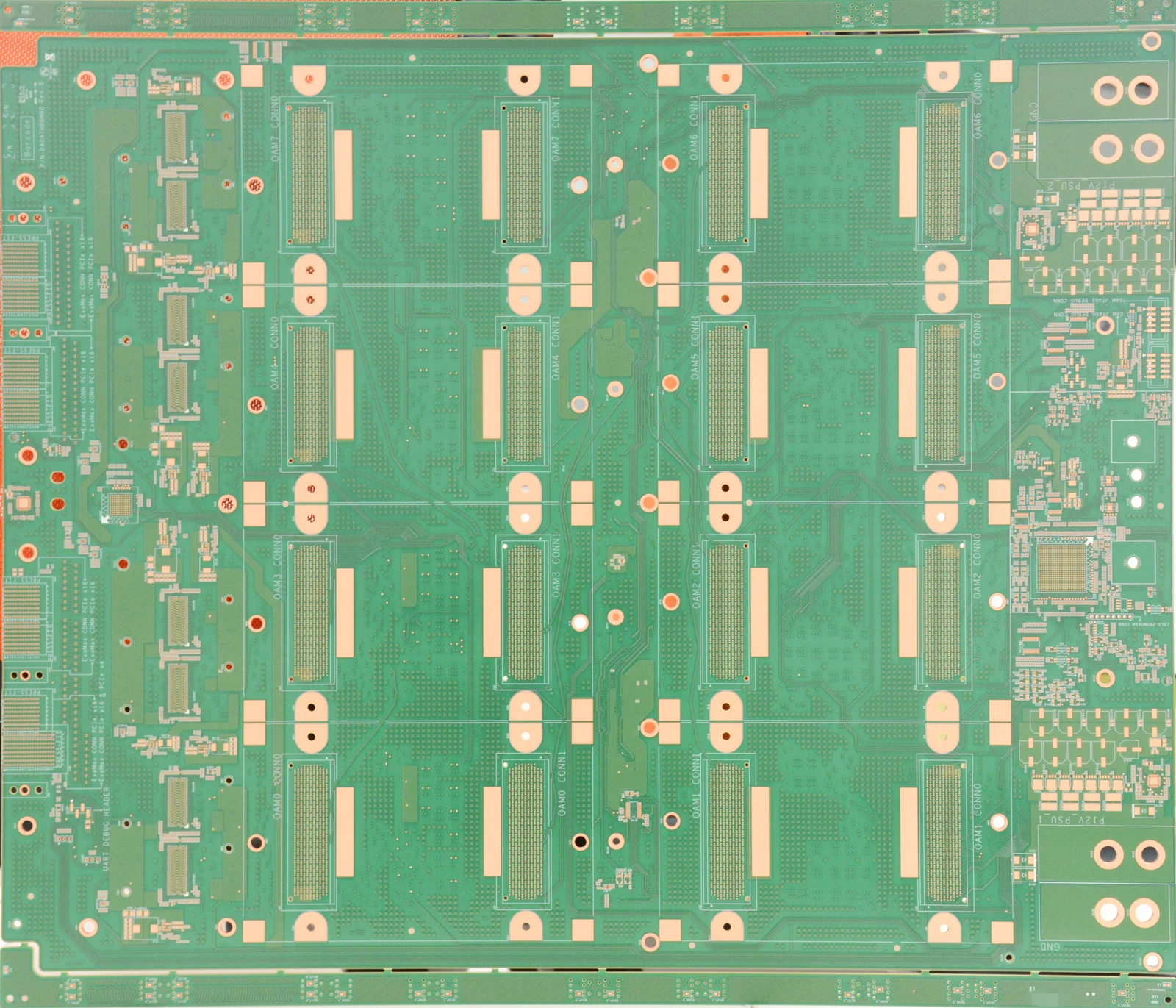
- Typical layers / thickness
- ≥20 / ≥3 mm
- Minimum drilled hole
- 0.2 mm
- Thickness / hole ratio
- ≥15:1 in the description
- Typical format wording
- Above 400 × 500 mm
- Trace / space
- 0.09 / 0.09 mm
- Selected impedance requirements
- ±8%
The page describes ultra-low-loss material and back drilling, resin fill and POFV for many designs. The size is typical descriptive wording, not an exact dimension of the photograph or a factory maximum. Likewise ±8% applies to some requirements in the source, not every net.
Identify module connector footprints, BGA regions, power-plane copper and thermal/mechanical constraints on the same released stack. Ask for layer-dependent registration, finished-hole and planarisation limits, the accepted large-format panel route and first-article measurement records. Do not combine this example’s size with a different page’s hole or trace extreme.
Make the first technical exchange usable.
Send a channel-aware fabrication pack.
Include the netlist, stack, artwork, outline and drill/back-drill tables. Classify signal paths by loss and impedance acceptance, identify material/foil/mask grades and include coupon and measurement definitions. Attach the connector drawings and any press-fit or module-interface constraints.
Return a site-specific process proposal.
Request the proposed fabrication and drilling locations, process exceptions, stack substitutions and inspection route. The website’s Guangzhou sales page currently lists patrick.yang@delton.com.cn and j.wang@delton.com.cn. This corrects the older general mailbox in the research record; no email-delivery test or outbound message has been performed.
Check the applicable qualification scope.
The current website’s quality image distinguishes Guangzhou, Huangshi and Thailand. For example, it prints Guangzhou IATF 0474393 and CNAS L21463 for the Guangzhou testing centre, while its IATF row has no Thailand entry. These are manufacturer-published references, not independently verified certificates here. Obtain current certificates, legal entity, expiry, site and testing scope for the actual order.
Agree the records delivered with the lot.
Specify laminate/foil lot traceability, electrical-test and netlist revision, sections, hole/slot dimensions, back-drill records and channel coupons. Define first-article approval and change notification before production. A photo, an equipment discussion or a group quality policy cannot replace these agreed shipment records.
Sources behind this profile
Individually read on 8 October 2026. Four original product photographs, the company-page exterior, the quality images and annual-report pages 8, 16 and 27 were visually examined. Catalogue constructions, newer dated group disclosures and quotation requirements retain separate scopes. Manufacturing illustrations do not prove customer approval, measured loss or independent certification.
- MANUFACTURER / ENTITYCurrent company identity and manufacturing-base description ↗
- MANUFACTURER / CONTACTGuangzhou addresses and current sales mailboxes ↗
- MANUFACTURER / SERVERDecember 2022 PCIe 5.0 example and process discussion ↗
- MANUFACTURER / SWITCHDecember 2022 hybrid-lamination switch example ↗
- MANUFACTURER / STORAGEMay 2024 storage backplane and connector processes ↗
- MANUFACTURER / UBBMay 2024 UBB construction and complete original photo ↗
- MANUFACTURER / QUALITYSite-separated certificate-reference and policy images ↗
- ISSUER / ORIGINAL REPORT2025 annual report: legal identity, updated process status and subsidiaries ↗