Dongguan circuits for contacts, flexible connections and compact assemblies.
Dongguan Cojoin Circuits Co., Ltd. · 东莞市科佳电路有限公司 publishes rigid, flexible and rigid-flex PCB examples alongside packaging-substrate and sensor galleries. Its contact page places the business in Nanzha Fourth Industrial Area, Humen, Dongguan, Guangdong.
The company's history dates its establishment to June 2010 under the name Dongguan Kangzhuang Circuits, followed by a rename to Cojoin in April 2015. It records separate rigid and flexible business units from July 2021. These dates come from its own history; the Hong Kong company also mentioned there is a separate entity.
For a sourcing decision, three details matter more than a single “PCB capability” number: which plated surface meets the component, where the flex is allowed to move, and which operations and tests are included in the delivery. The examples below retain their own construction and finish parameters.
CONTACT SURFACES / THREE RIGID EXAMPLES
Specify the finish by its function.
Cojoin's rigid-board catalogue differentiates immersion tin, electroplated nickel/gold and ENEPIG. The plated contacts and wire-bonding surfaces should be assessed against the mating component and assembly process, rather than grouped under “gold finish”.
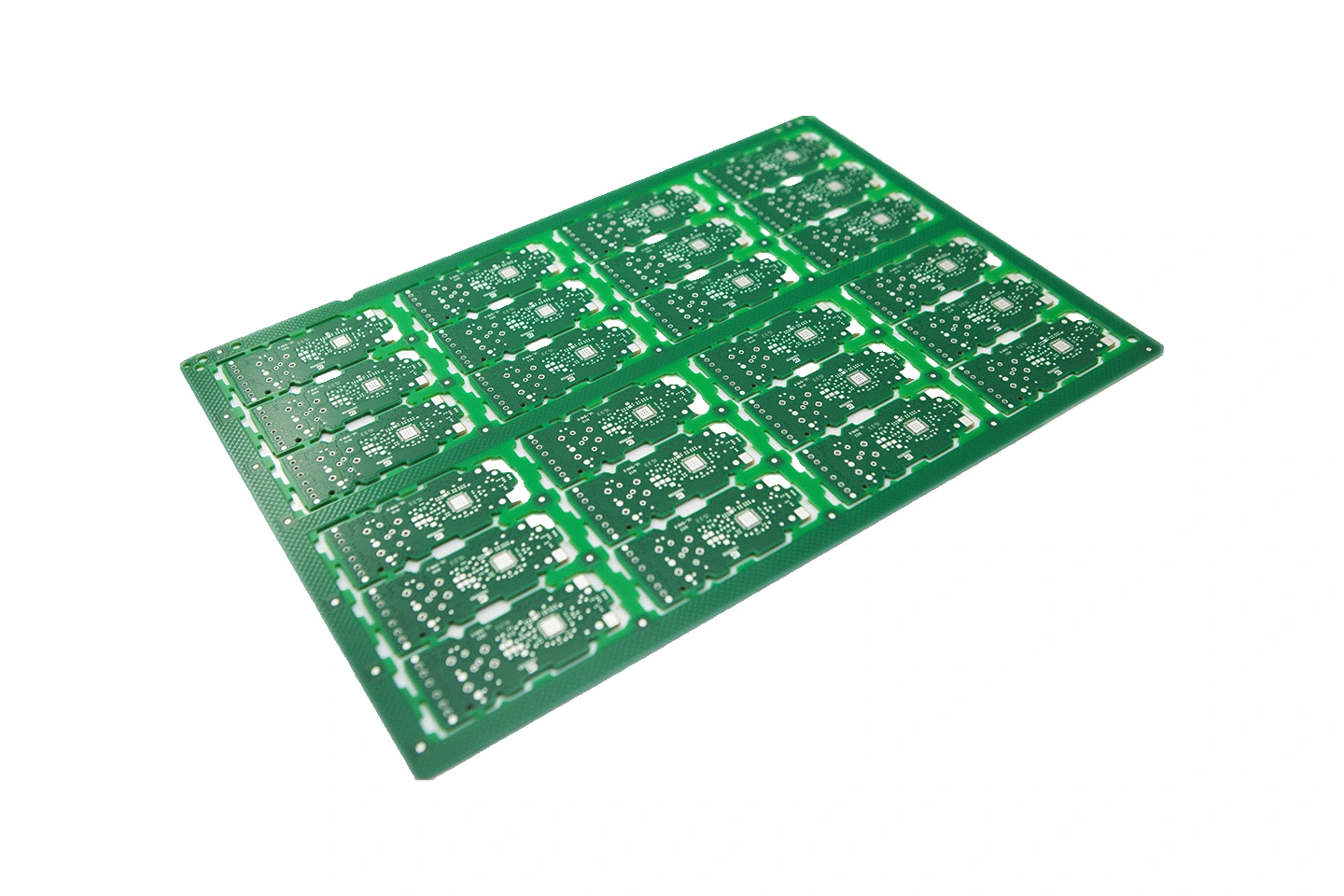
Original product-page image · 汽车车窗控制板
Vehicle-window control PCB
Layers
4
Trace / space
0.4 / 0.4 mm
Published minimum hole
0.3 mm; drill/finished basis unspecified
Finish
Immersion tin
Release connector holes, panel and mounting drawing, copper and the tin-finish acceptance. Automotive application wording alone is not programme qualification.
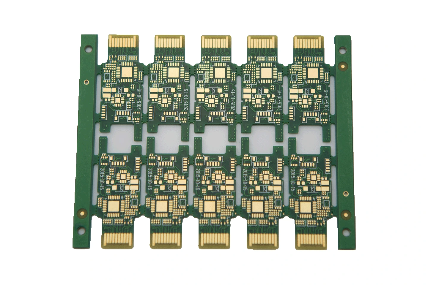
Original product-page image · 光电传输转接板
Optoelectronic transmission adapter PCB
Layers
4
Trace / space
0.3 / 0.3 mm
Published minimum hole
0.2 mm; basis unspecified
Electroplated finish
Ni 3–8 μm / Au 0.38–0.76 μm
Additional features
Impedance control; bevelled gold-finger edge
Specify the contact area, bevel geometry, mating-cycle requirement and impedance stack/target/tolerance. The source provides no numeric impedance tolerance.
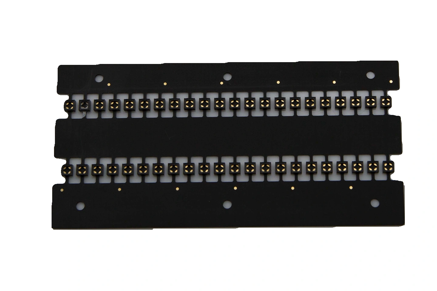
Original product-page image · 汽车尾气传感器
Exhaust-sensor cavity PCB
Layers
4
Trace / space
0.2 / 0.2 mm
Published minimum hole
0.2 mm; basis unspecified
ENEPIG finish
Ni 3–8 μm / Pd 0.05–0.15 μm / Au 0.05–0.15 μm
Structural/process wording
Cavity; gold-wire bonding wording
Send the cavity dimensions, bond-pad geometry, bond process and pad acceptance. Clarify whether the delivery includes bonding or only a board intended for bonding.
What the catalogue's hole value means
The individual pages publish minimum hole diameters, but do not define whether they are drill diameters or finished plated holes. Their literal values are retained above; they are not entered as confirmed finished-hole limits in the directory filter. The optoelectronic example states impedance control without a numeric tolerance. Supply the actual stack, target, tolerance and coupon for engineering review.
The exhaust-sensor page writes “Cavity” in its special-material field and “金线banding” in its process field. Cavity is a structural feature, not a laminate brand. Confirm cavity geometry, bond-pad acceptance and whether wire bonding is a supplied operation or an intended downstream application.
FPC / GEOMETRY & FUNCTION
Two flexible examples, two different acceptance questions.
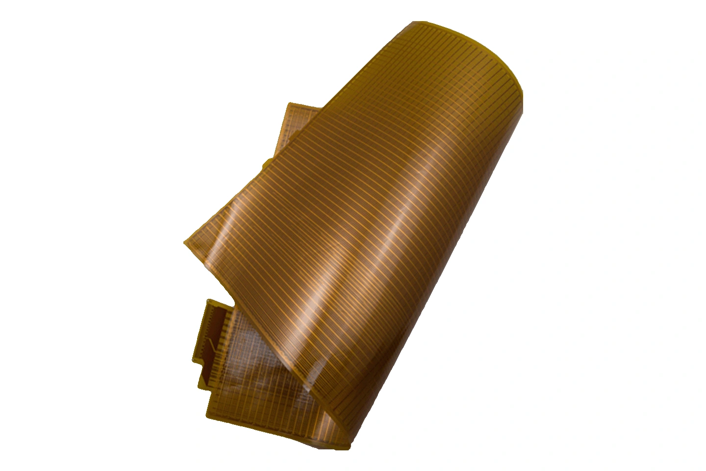
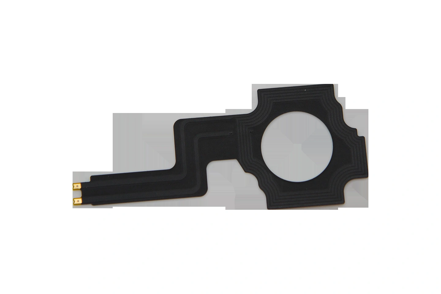
密集环形线路 · manufacturer catalogue
Dense annular flexible circuit
Layers
2
Trace / space
0.075 / 0.075 mm
Published minimum hole
0.1 mm; basis unspecified
Finish
Electroplated nickel/gold
Release flex laminate, copper, coverlay openings, installed bend and cycle-life criteria. The fine-line figure belongs to this two-layer example.
NFC支付天线 · manufacturer catalogue
NFC payment antenna circuit
Layers
2
Trace / space
0.2 / 0.2 mm
Published minimum hole
0.3 mm; basis unspecified
Finish
Electroplated nickel/gold
Additional processing
Abrasion-resistant ink; salt-spray wording
Define the antenna/circuit drawing, tuning and assembly interfaces, ink wear acceptance and salt-spray duration/criteria. No read range or RF performance is published.
The dense annular circuit is the finer-line example in this selection: 0.075/0.075 mm. That is a parameter of this two-layer product, not an across-the-board promise for an eight-layer rigid-flex construction. Both FPC pages omit the laminate grade, copper, thickness, minimum bend radius and cycle-life acceptance; send these explicitly.
RIGID-FLEX / RELEASE THE ZONES
Layer count needs a construction drawing.
The industrial conversion board, camera-module board and medical magnifier control board have different flex structures and surfaces. Treat each as a separate design route. A medical application name does not establish an ISO 13485 certification or a medical-device approval.
工业类转换控制板 · original product photograph
Industrial conversion-control rigid-flex PCB
Layers / construction
4 layers; flex cut-out
Trace / space
0.15 / 0.15 mm
Published minimum hole
0.2 mm; basis unspecified
Finish
OSP
Reinforcement
PI; not a complete laminate specification
Define rigid/flex zones, cut-out dimensions, PI stiffener and adhesive, coverlay and the assembled bend. Ask for the actual section drawing.
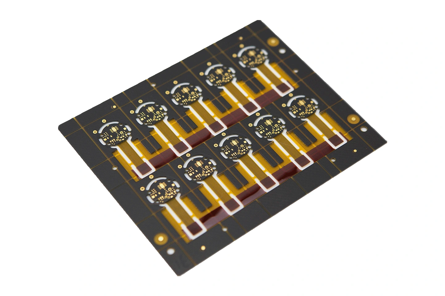
手机摄像头模组 · original product photograph
Camera-module rigid-flex PCB
Layers
4
Trace / space
0.2 / 0.2 mm
Published minimum hole
0.2 mm; basis unspecified
ENEPIG finish
Ni 3–8 μm / Pd 0.05–0.15 μm / Au 0.05–0.15 μm
Construction
Shielding film and conductive adhesive; gold-wire bonding wording
Specify shielding-film grounding, conductive-adhesive contact, flex transitions and bond-pad acceptance. Confirm board-only versus bonding/assembly scope.
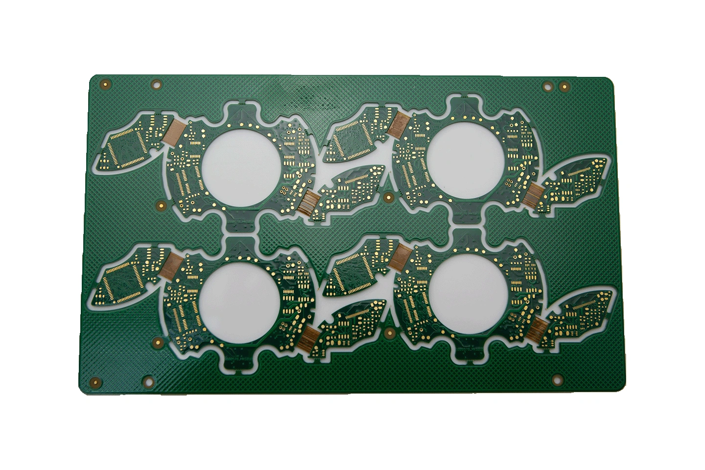
医疗设备放大镜控制板 · original product photograph
Medical magnifier-control rigid-flex PCB
Construction
8 layers: 2 FPCB + 6 PCB
Trace / space
0.2 / 0.2 mm
Published minimum hole
0.3 mm; basis unspecified
ENEPIG finish
Ni 3–8 μm / Pd 0.05–0.15 μm / Au 0.05–0.15 μm
Process features
Blind/buried vias; gold-wire bonding wording
Release the full zone-by-zone stack, via map, coverlay, bend and test plan. The medical application name is not a device approval or ISO 13485 claim.
Engineering review before a rigid-flex quotation
Provide a section drawing for each rigid and flex zone, copper distribution, coverlay openings, transition geometry, stiffener material and adhesive. For movement, state the assembled bend and whether it is static or repetitive. For the camera example, define shielding-film grounding and conductive-adhesive interfaces. For the eight-layer example, the published “2 FPCB + 6 PCB” description still needs an actual stack and via map.
The source gives no numeric impedance tolerance or bend-cycle qualification for these examples. Request a construction-specific assessment; do not combine the annular FPC's fine-line figure with the medical board's layer count.
PACKAGING / A DIFFERENT DATA PACKAGE
The substrate gallery is a starting point for a packaging review.
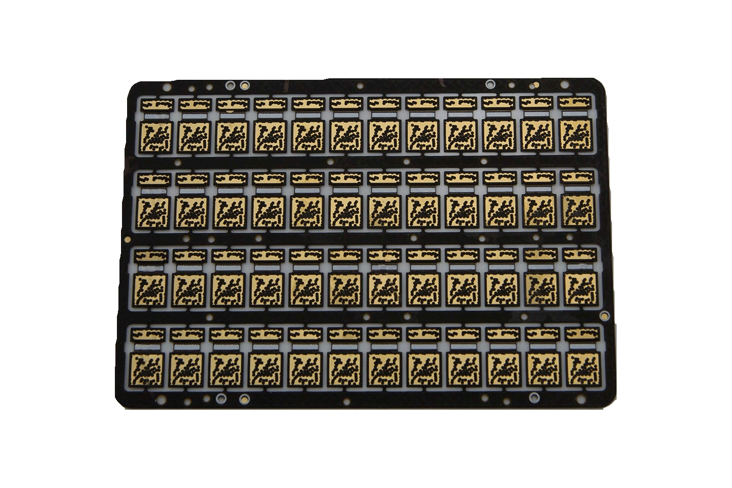
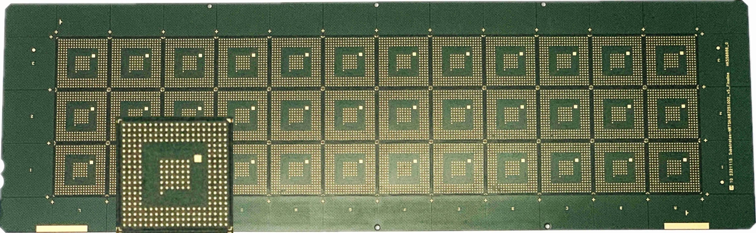
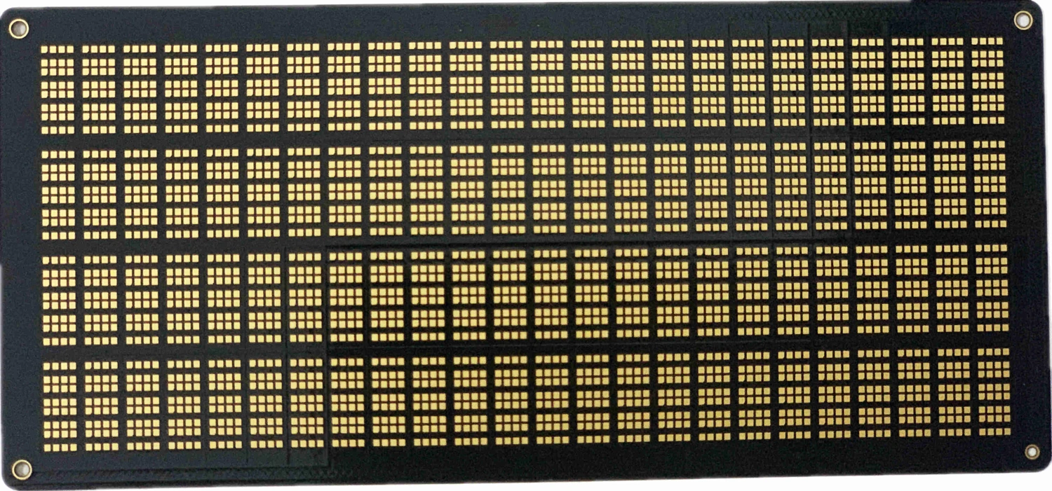
Official catalogue entry “载板16”. The number is its title, not a published layer count.Official catalogue entry “载板21”. Its specification fields are empty.
Substrate enquiry inputs
These two pages supply original images but no layer count, pitch, substrate grade, copper, warpage limit or delivery format. Submit die/package drawings, pad and bond-area requirements, substrate construction, finish thickness, panel map and assembly-temperature profile. Ask for the proposed process window and its measurement plan before shortlisting a numeric capability.
Keep substrate fabrication, die attachment, bonding and encapsulation as separate responsibilities. The gallery alone does not establish that Cojoin supplies a complete packaged semiconductor.
PROCESS / IMAGING, PLATING & RELEASE
Match the production route to the inspection plan.
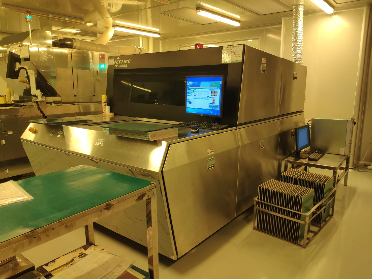
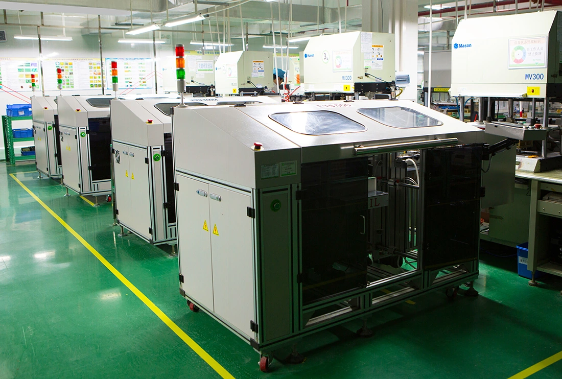
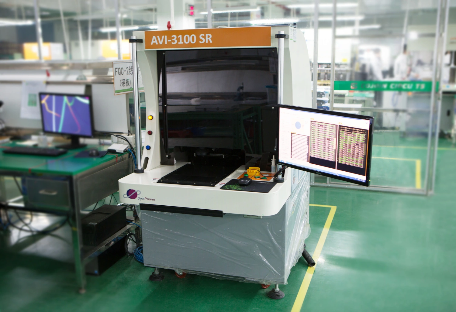
The manufacturer's equipment gallery labels direct laser imaging, semi-automatic DI exposure, drilling, copper/tin plating, electroless copper, VCP plating, OSP, automatic electrical testing, AVI visual inspection and automatic measurement. These are source-labelled equipment photographs; they do not establish machine ownership, current utilisation or a site-audit result.
Laser direct imaging — source label.Automatic ET testing — source label.AVI visual inspection — source label.
What its quality page describes
The quality page describes APQP, PPAP, SPC, MSA and FMEA, customer criteria alongside IPC Class 2, and 100% open/short and visual inspection. It also names Cu/Ni/Au thickness checks, solderability, dimensions and microsection inspection. These are manufacturer-reported practices, not independently observed batch results.
What your purchase order should settle
Agree netlist revision, electrical-test coverage and report format; plated thickness locations and sampling; microsection coupons and acceptance; and the final visual class. The site's Class 2 wording is not a Class 3 commitment. Reliability tests listed include thermal stress/shock, ionic contamination, salt spray and humidity; select conditions and reports for the actual construction.
QUALIFICATION / FIRST ORDER
Release the construction, then the programme.
Choose a specific example or construction. Attach the stack, flex-zone drawing, cavity/via map or package interface.
Define the functional surface. Contact or bond-pad finish, thickness, geometry, shielding and assembly interface.
Agree the acceptance package. Hole definition, electrical test, plating measurement, coupons, inspection class and construction-specific reliability tests.
Confirm the delivery scope. Bare board versus assembly, any external processes, supplying address, quantity, material reservation, lead time and lot records.
Obtain current qualification records. Match the entity, addresses, scope and validity to the programme; automotive and medical application labels are not approvals.
The official contact page publishes sales@cojoin.com.cn. Andy Lan is named for the global market, and the support page uses andy.lan@cojoin.com.cn for technical support. Mailbox publication was checked; mailbox control was not tested. Continue the enquiry within PCBVerified through the relevant shortlist action.
The manufacturer-hosted copy identifies Dongguan Cojoin Circuits Co., Ltd., No. 14-1 First Street, Xinxing Road, Nanzha, Humen. It shows IECQ-H SGSCN 22.0056, issue 3, issued 9 September 2025 and expiring 8 September 2028, for manufacture of rigid, flexible and rigid-flexible PCBs.
The image specifies QC 080000:2017; the webpage title says “QC080000:2025”. The certificate's own wording is retained. Its printed “Current” status is a statement on that copy; live IECQ register status was not established in this review. This is hazardous-substance process management, not proof that a particular lot passed your material test.
Read the older ISO and IATF copies
The ISO 14001 copy CN12/30098 runs to 10 January 2024. The ISO 9001 copy CN13/30582 runs to 31 May 2024. The IATF copy identifies IATF 0402774 / SGS CN13/30581 and also runs to 31 May 2024, excluding product design clause 8.3.
Those published copies are historical at this review date. They have not been presented as current badges; request renewed documents with the supplying site's scope before an automotive or other controlled programme.
The original national standards record provides independent context for the legal name and drafting role. The product values, equipment photographs and qualification copies above remain attributed to the manufacturer. No UL holder or batch-level material-traceability record was established.
SOURCE TRAIL
Sources behind this profile
Individually reviewed 9 October 2026. Eleven original product pages and photographs, the equipment gallery, seven process diagrams, qualification copies and the national standards record were read. Eight numeric board examples remain distinct; packaging and sensor pages have no invented specifications. Minimum-hole entries are not confirmed finished-hole values. Printed certificate dates and the IECQ title/version discrepancy are preserved.