CHENGZHIYI / HEAT PATH, ELECTRICAL ISOLATION AND COPPER GEOMETRY
A copper base, a copper insert and thick circuit copper solve different problems.
Shenzhen Chengzhiyi Circuit Co., Ltd. · 深圳市诚之益电路有限公司 describes a business established in August 2008, with Shenzhen research/technical contact and production locations in Dongguan and Ji’an. Its portfolio is particularly relevant to automotive lighting and power-control designs where heat has to leave a component without shorting the circuit to its metal base.
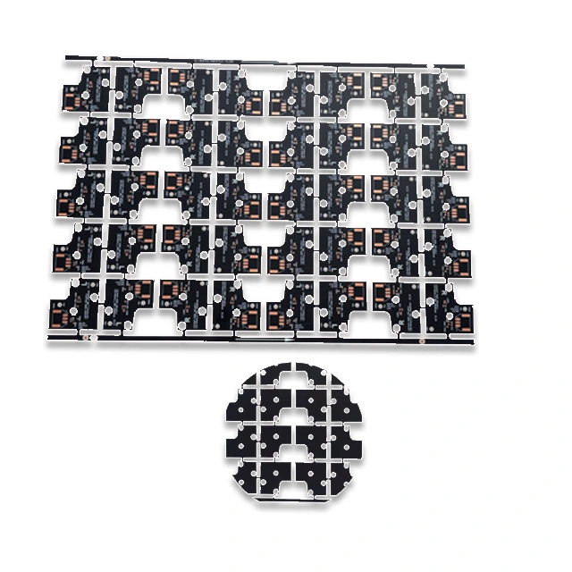
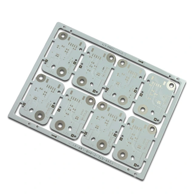
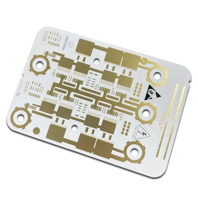
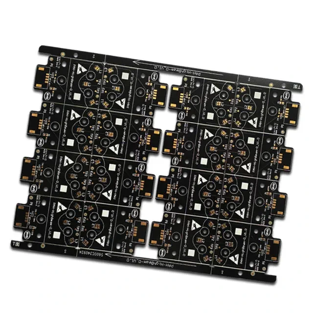
The 16 examples below each use their corresponding original catalogue image. Most metal-base pages identify a construction but do not provide a complete stack: the detailed anodised-aluminium and six-layer FR-4 examples are therefore separated from title-only references.
METAL-BASE BOARDS / FOLLOW THE HEAT WITHOUT LOSING ISOLATION
Begin with the thermal interface drawing.
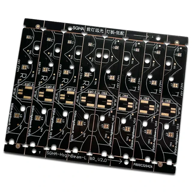
The anodised automotive-lighting example publishes a useful combination: 1.6 mm, 2 oz, 3 W/m·K and OSP. That does not establish dielectric thickness, a laminate brand or the thermal resistance of the mounted assembly. Its black anodised back treatment must also be distinguished from the circuit surface finish.
Anodised aluminium automotive-lighting board
Thickness / copper
1.6 mm / 2 oz
Dielectric thermal conductivity
3 W/m·K
Surface / finish
Matte black mask, high-reflectivity anode wording / OSP
Back treatment
Black anodisation of aluminium
Specify dielectric grade and thickness, isolation voltage, heat-sink interface and anodisation masking. The source gives no quantified improvement from the back treatment.
Copper-base immersion-tin board
Finish
Immersion tin, as named in the title
Thermal title
8W; full conductivity unit and test basis absent
Ask for the dielectric thermal conductivity in W/m·K, finished thickness and immersion-tin acceptance. Do not substitute HASL or interpret 8W as operating power.
Single-sided two-layer copper-base example
Source title
Single-sided two-layer copper-base board
Stack definition
Two-layer wording needs a layer-by-layer drawing
Clarify the circuit-layer count versus base/thermal layers, vias between conductors and insulation around exposed thermal pads. Two-layer title alone does not approve a build.
The “122W” field is not a released power rating
The thermal-separation aluminium page writes “122W” in its title, while its model field says copper/aluminium composite. The technical table likewise uses incomplete thermal units, including “398W” beside separation wording. Neither a wattage capacity nor a W/m·K value has been inferred. Ask for the material/system value, units, measurement method and exact stack revision.
Thermal/electrical separation aluminium-base example
122W is incomplete; not a power or W/m·K specification
Resolve the model and stack drawing: where is the direct thermal connection, which regions stay electrically isolated, and how is interface resistance tested?
Copper/aluminium composite base-board example
Base route
Copper/aluminium composite, as titled
Missing construction data
No copper insert dimensions, bond or dielectric grade
Specify the copper-to-aluminium joint, flatness, electrical clearance and the thermal test for the assembled interface; do not treat the photo as a released stack.
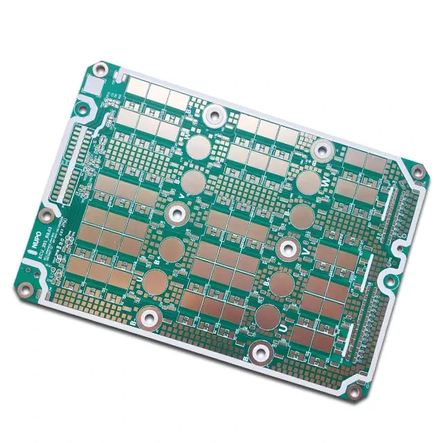
High-power electronic-control copper-base board
Application title
High-power electronic control
Model field
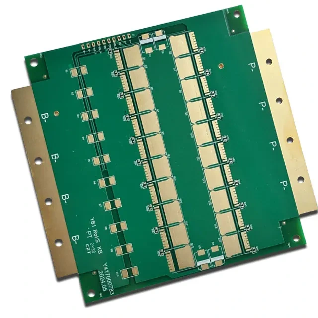
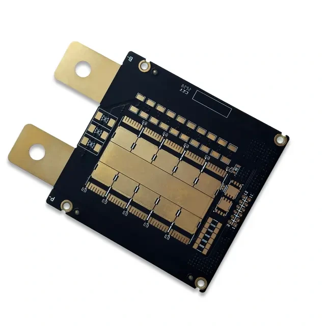
New-energy electronic-control thick-copper board
Limits
No product-specific layer, thickness or current rating
Send component power loss, copper design and the mechanical heat-sink interface. This photograph and application name do not define a safe operating current.
No instance-specific finished copper or current value
Agree finished copper distribution, press/etch route and isolation from the base. The two control-board pages use a similar model name but show different original examples.
The two electronic-control pages show distinct boards despite similar model wording. A “new-energy” or “high-power” title does not specify battery voltage, continuous current, isolation category or an approved automotive programme.
INSERTS AND HEAVY COPPER / RELEASE GEOMETRY BEFORE A CURRENT TARGET
The insert joint is part of the board specification.
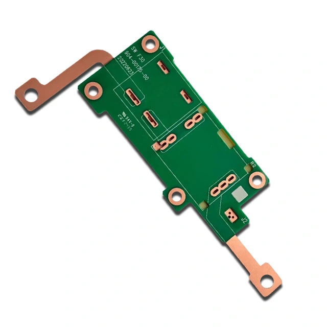
An embedded copper block can provide a local heat path or current connection; thick etched copper changes the circuit cross-section. They need different dimensions, bonding and inspection instructions. Chengzhiyi shows both routes, plus separate drone application examples.
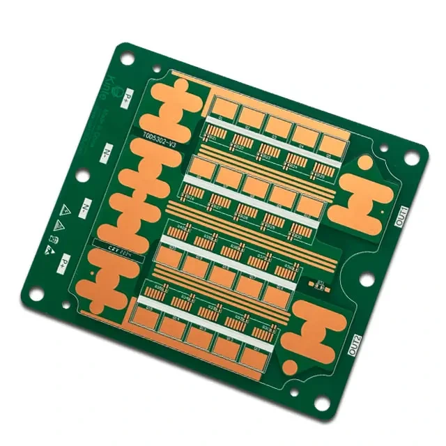
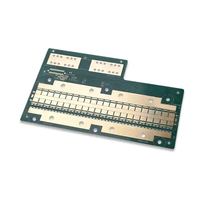
9 oz industrial-controller thick-copper circuit
Copper title
9 oz
Application
Industrial controller
Thickness / layers
Not separately published for this example
State whether 9 oz means starting foil or finished copper, allowable etch profile, trace spacing and temperature rise. Release the actual stack and finished current-carrying cross-section.
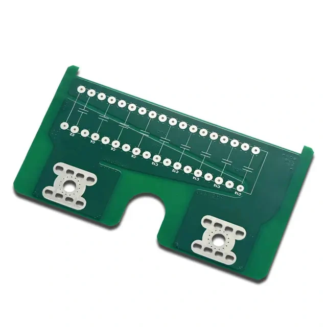
Embedded-copper PCB example
Construction title
Buried/embedded copper PCB
Insert information
No thickness, bond, position or thermal resistance
Supply the insert drawing, tolerance and datum, connection to circuit copper, bonding process and acceptance after thermal cycling.
Copper-insert double-sided copper-base board
Source title
Copper insert, double-sided copper-base board
Geometry
Insert and dielectric thickness not published
Define both electrical faces and the copper-block interface, insulation around the insert and the expected mounting/thermal load. The title establishes the route, not all dimensions.
Ask for the section through the insert
Include insert thickness and position, protrusion/recess tolerance, bond region, conductor connection, insulation clearance, thermal expansion and test after the specified cycling. Agree who supplies and machines the insert, which surfaces receive a finish, and the inspection datum. A current target needs ambient and allowed temperature rise, duty cycle and the finished conductor geometry.
FPV-drone embedded-copper example
Application title
FPV-drone copper-insert PCB
Electrical rating
No published current, battery or power rating
Give transient current, connector geometry, thermal losses and required isolation. Do not infer battery voltage or motor rating from visible pads.
Drone copper-block PCB example
Application title
Drone copper-block PCB
Engineering data
No layer, insert dimensions or current specification
Release copper-block dimensions and connection method, mechanical support and thermal acceptance. This is a distinct source image, not a second certification or tested drone design.
RIGID-FLEX AND BLIND/BURIED VIAS / STACK SEQUENCE MATTERS
Do not combine a layer title with the smallest row in the process chart.
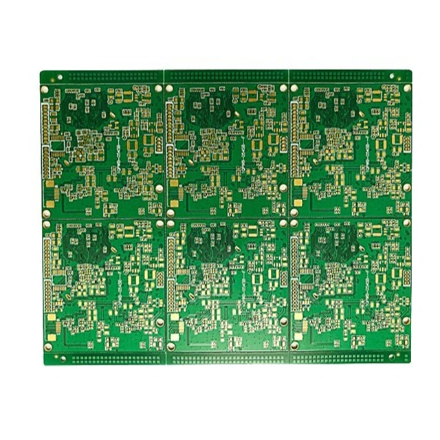
Six-layer blind/buried-via FR-4 board
Layers / thickness
6 / 1.2 mm
Copper / finish
1 oz / immersion gold
Line / space
0.065 / 0.065 mm
Hole wording
Minimum 0.15 mm; finished-hole definition absent
Confirm the blind/buried-via sequence, dielectric grade, hole basis and plating/filled-via acceptance. The 0.15 mm wording is not entered as a finished plated-hole filter.
The six-layer FR-4 example explicitly supplies 0.065 mm line/space, 1.2 mm thickness, 1 oz copper and immersion gold. Its 0.15 mm minimum-hole phrase does not distinguish drilling from a finished plated hole. The directory keeps that finished-hole value unknown, and the via sequence still needs a released stack.
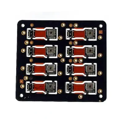
Four-layer copper-base rigid-flex example
Source title
Copper-base rigid-flex board, four layers
Flex construction
No polyimide, bend radius or cycle specification
Request the rigid/flex/metal-base cross-section, copper transitions and bend condition. The generic rigid-flex chart is not a four-layer copper-base approval.
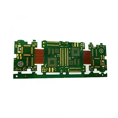
Eight-layer rigid-flex catalogue example
Layer title
8 layers
Construction data
No instance-specific dielectric or flex lifetime
Ask which layers continue through the flex region, stiffener position, coverlay openings and bend validation with the assembled connectors.
24-layer rigid-flex catalogue example
Layer title
24 layers
Construction data
No instance-specific line, hole or bend limits
Release layer distribution across rigid and flexible regions, press cycles, via arrangement, final thickness and whether flexing is installation-only or repeated.
Manufacturer's general rigid-flex table
Board thickness rows
Minimum 0.05 ±0.03 mm; maximum 8 mm
Largest processing size
485 × 1500 mm
Minimum line / space
0.025 / 0.025 mm
Minimum hole / aspect ratio
0.05 mm, basis unspecified / 12:1
PI film options
0.5, 0.8, 1, 2 and 3 mil
ED / RA copper options
¼, ⅓, ½, 1 and 2 oz
Release the flex region separately
The chart lists PI, FR-4, steel and aluminium stiffeners, coverlay and several named material suppliers. These are general options; none is assigned to the 4-, 8- or 24-layer photo without the specific stack and bill of materials.
The impedance row uses ±5 Ω for 0–50 Ω and ±10% above 50 Ω, with an overlapping boundary at 50 Ω. It is not an across-the-board ±5% promise. Clarify the boundary, coupon, frequency and acceptance measurement.
Specify static installation versus repeated bending, bend radius, copper type, region-by-region layer count, coverlay opening, stiffeners and the assembled bend test. No flex lifetime is inferred from these images.
PROCESS AND TEST RELEASE / GET THE OUTPUT WITH THE ORDER
Match the production route to a measurable acceptance record.
General metal-base chart
Base / copper
Aluminium or copper / 1–12 oz
Substrate thickness
0.2–5 mm
Minimum line / space
0.10 / 0.10 mm
Minimum hole
0.25 mm; no finished-hole definition
Largest / smallest work size
1500 × 500 mm / 5 × 5 mm
AC withstand row
1500–4000 V; duration and leakage criterion unspecified
Agree what is measured
The general page names CNC, punching, V-cut and laser profiling; another company paragraph gives a broader 0.17–6 mm research/production range. These are different source scopes, not a guaranteed 6 mm board at the largest size.
For a metal-base order, agree final outline, base and dielectric thickness, finished copper, plating/finish, electrical netlist, isolation test and thermal test method. Specify the document linked to the batch and engineering revision.
Published sample and batch lead-time rows are 3–4 and 5–6 days. Confirm quantity, material availability, engineering approval, inserts and final test before treating them as an order schedule.
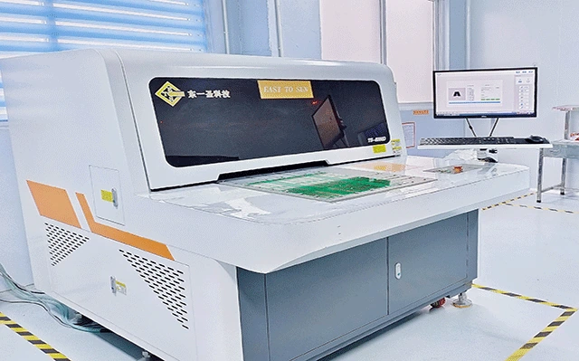
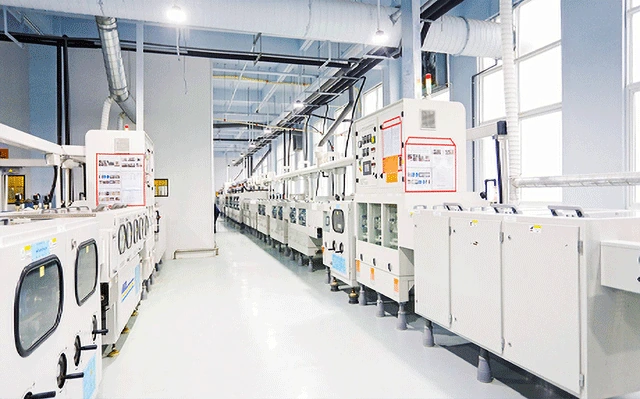
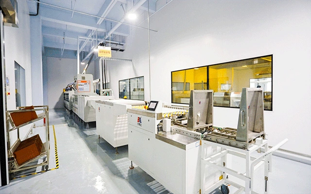
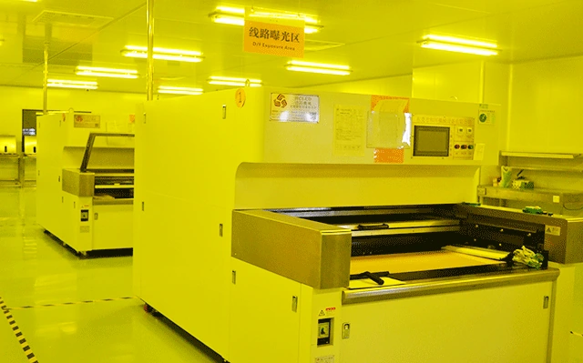
The dedicated equipment page labels printing, DES, tunnel baking, mask developing, LED exposure, automatic receiving, ovens and targeting equipment. Newer product pages additionally describe CCD drilling, VCP plating, vacuum pressing, LDI/CCD/LED exposure, AOI, E-test, four-wire test and AVI at Jiangxi. These are manufacturer's published descriptions; the dedicated exposure photo does not independently establish an LDI model or machine availability.
CONTRACTED ENTITY, PLANT AND DATED RECORDS
Put the actual production entity on the quote.
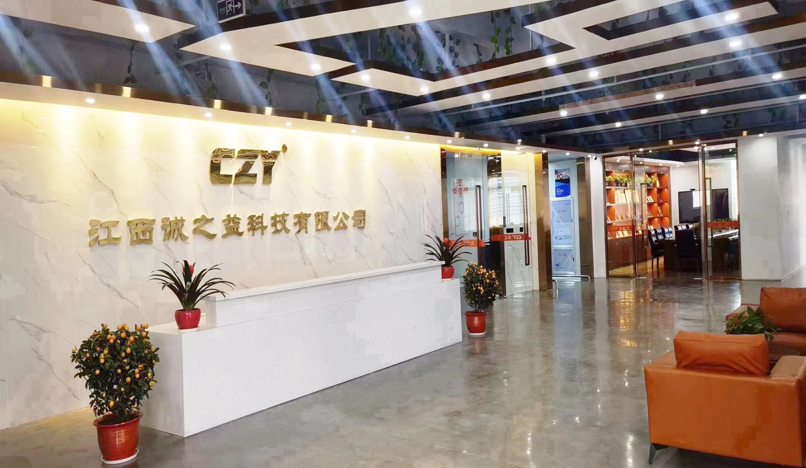
The official company page's Jiangxi reception photograph. It does not establish the condition or capacity of every production line.
Shenzhen research / company contact
8A, Quanzhi Technology Innovation Park, Houting, Shajing, Shenzhen.
Dongguan production address
Floors 1–4, Building A, Fenghuangshan Environmental Industrial Park, Shajiao, Humen.
Jiangxi production address
Building A6, Heying Industrial Park, Shuangxiu Road, Jizhou industrial park, Ji’an.
Officially published contact
+86 755 81736919 · market@czypcb.com
The website names 江西诚之益科技有限公司 and states mass production began in March 2022. Its reported 25,000 m² and 100,000 m²/month expansion figures are undated design/expansion descriptions, not reserved capacity. Request the entity, plant and routing actually responsible for the quote.
CNIPA's complete 4 March 2020 notice names 深圳市诚之益电路有限公司 as right holder for BS.195627482, “铜基板热电分离加工设备电路设计布图”, with the Shenzhen 8A address. This is a dated integrated-circuit layout-design record, not a PCB performance test or current qualification.
Dated manufacturer-hosted documents and their exact scope
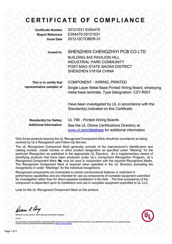
The UL copy is issued 31 October 2012, certificate 20121031-E354470, for representative single-layer metal-base boards, designation CZY-R001. The historical address and specified scope must not be extended to all current plants or rigid-flex boards. Current file ownership, construction listing and site scope need the issuer's current record.
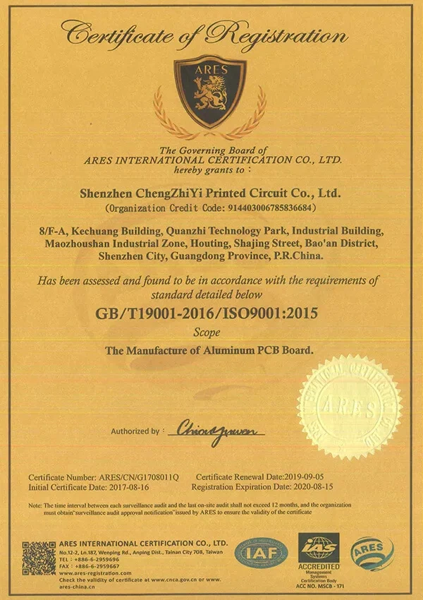
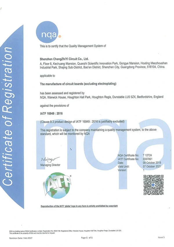
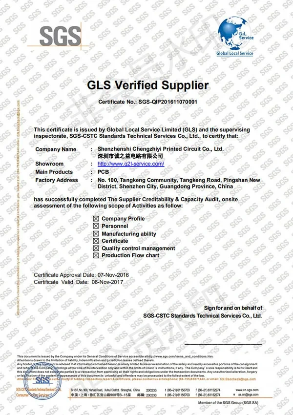
The ARES ISO 9001 copy ARES/CN/GI1708011Q describes aluminium PCB manufacture and expires 15 August 2020. NQA IATF T12724 / 0337861 excludes electroplating and product design; its printed validity ends 7 October 2021. The GLS/SGS supplier-assessment copy SGS-QIP201611070001 expires 6 November 2017 and gives a historical Tangken address. None is shown as a current certification badge.
2012 UL representative construction copyHistorical ARES ISO 9001 copyHistorical NQA IATF copy2016 GLS supplier assessment copy
For qualification, request the renewed issuer record, the manufacturing-address scope, approved construction/material and product acceptance plan. Website email was read as a contact source; mailbox control has not been tested and no message was sent.
SOURCE TRAIL
Sources behind this profile
Individually researched 9 October 2026: original company, contact, technical tables, equipment and division pages; 16 product pages and their separately examined corresponding original images; dated qualification copies; complete CNIPA notice with the exact Shenzhen legal entity. General table values, incomplete thermal units and historical certificates retain their own scope.