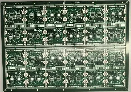
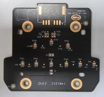
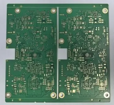
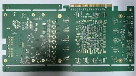
What must the board carry: heat, power or a signal?
Chanyee is the website and catalogue brand of 诚亿电子(嘉兴)有限公司, Chengyi Electronics (Jiaxing). Its company introduction dates the business to 2004 and describes development and manufacture of high-density rigid printed circuit boards. The official contact address is No. 972 Gangshan Road, Jiaxing, Zhejiang. Its catalogue is particularly useful where copper geometry does more than connect components: an embedded block moves heat, a protruding copper feature defines a mechanical interface, and a multilayer winding becomes part of a transformer.
These are different fabrication routes. The layer range beside each family is the manufacturer’s published offering for small and large batches, not a measured layer count for every photographed board. Select the construction first, then agree one stack and acceptance package for the order.
HEAT PATHS / TWO COPPER GEOMETRIES
Embedded copper and protruding copper are separate products.
Official buried-copper catalogue image. The internal cross-section is not visible.
Embedded block · 2–8 layers
The buried-copper page describes a metal copper block embedded in the PCB, with a 2–8-layer offering for small and large batches. Applications named include 5G equipment, high-performance computing, automotive electronics, industrial controls and energy storage.
Release block dimensions, position and connection to the component’s thermal pad. Ask whether the block is exposed, electrically connected or insulated at each face, how the interface is bonded, and what coplanarity the assembled heat path requires. A block inside a laminate is not automatically a zero-insulation direct-thermal path.
Official copper-convex family photo. Protrusion height and interface flatness require a drawing.
Protruding copper · 2–4 layers
The copper-convex page describes a copper structure protruding from the board surface, alongside an insulating substrate and copper-foil circuitry. Its stated range is 2–4 layers in small and large batches, with headlights, daytime running lights and fog lights as examples.
Define the protrusion’s datum, height, lateral tolerance, contact area and surface condition. The mating LED or thermal assembly needs an agreed seating plane and attachment method. Ask how the protruding region is inspected and protected during handling; do not substitute the embedded-block dimensions from another family.
The thermal number must belong to an assembly.
Neither family page supplies block tolerance, thermal resistance, copper weight, dielectric grade or a measured junction-to-heatsink result. Specify power dissipation, heat-source footprint, insulation requirement, interface material and heatsink conditions. Agree whether acceptance uses dimensional inspection, microsection, bond integrity or a representative thermal test. The catalogue images establish the offered families; they do not establish performance at a buyer’s operating point.
POWER / PCB AS A WINDING STRUCTURE
The layer count does not define the transformer.
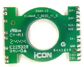
Official planar-transformer catalogue photo. The 6–16-layer range describes the offered family.
Chengyi lists planar-transformer PCB manufacture in small and large batches for 6–16 layers. The page describes multilayer PCB windings used with a ferrite magnetic component and gives applications in communications, lighting, computers, industrial equipment and fast charging. That is a winding-board fabrication route; it does not establish supply of a complete transformer or a particular magnetics rating.
Published family range
6–16 layers
Winding release
Layer connections, turns and current paths
Insulation release
Primary/secondary separation and dielectric stack
Send the winding topology, copper per layer, terminal assignment, finished dimensions, core window and mechanical clearance. Define the primary-to-secondary isolation and creepage/clearance relevant to the assembled design. Agree the dielectric and electrical test specimen with the actual magnetic and thermal duty. The page’s general discussion of low resistance and low leakage does not give measured DCR, inductance, capacitance, frequency or power for the pictured board.
For a prototype-to-production transition, keep the approved dielectric stack and copper schedule in the drawing rather than choosing a layer count alone. A substitution that preserves total thickness can still change winding resistance or the insulation construction. Ask which fabrication measurements and test records accompany the PCB, and which magnetic characteristics must be measured after assembly.
RADAR / RELEASE THE RF STACK
A six-to-eight-layer radar offering needs a grade-specific quote.
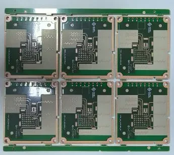
Original radar-family image. It is not a measured antenna or loss-test record.
The radar page states 6–8-layer fabrication for small and large batches. It describes PTFE high-frequency substrates and low-loss copper-clad laminates, naming Rogers and Panasonic as examples. The listed applications include automotive radar, security, industrial testing and road traffic.
These brand names do not identify the quoted grade, bonding sheet, material lot or supplier authorisation. Request the laminate system, RF layer positions, dielectric thickness and copper profile. Do not infer an exact operating band or grade from the circuit’s appearance.
Give the operating band, feed/antenna geometry, controlled-impedance requirements where applicable, finish and connector or solder interface. Ask how the factory controls etching, registration and relevant outline features on this construction. The source does not state a numeric minimum trace, plated-hole diameter, impedance tolerance or insertion-loss result for the family.
Release RF coupon geometry and test conditions, including fixture/reference planes, alongside the drawings. Decide whether acceptance concerns the bare PCB, a populated radar module or the integrated antenna system. Those are different measurement boundaries; a material data sheet cannot prove the completed system’s detection distance or accuracy.
DENSITY / VIA CONSTRUCTION AND CHANNEL CONTROL
HDI and GPU manufacture answer different first questions.
Official HDI family photo; no microvia diameter is inferred.
HDI · define the interconnect
The HDI page describes micro blind/buried vias and multilayer lamination and drilling, with small and large batches. It gives no numeric layer ceiling, laser-hole diameter or minimum routing. The embedded-copper 2–8 range and the radar 6–8 range are not HDI limits.
Provide the build-up drawing, via targets, stacked/staggered arrangements and fill/cap requirement. Request the laser-to-target registration, dielectric thickness and agreed interconnect reliability evidence. A count of layers alone cannot define the number of lamination cycles or the qualification coupon.
Official GPU-board family image; assembly and GPU device supply are not established by this page.
GPU board · 14–22 layers
The GPU product page lists small-batch and mass manufacture for 14–22 layers. Its AI background does not identify a specific GPU, supported data rate, laminate system, back-drill capability or assembled accelerator model.
Release the electrical stack, BGA escape, reference planes, channel-length requirements and any residual-stub specification. Ask for material substitutions and impedance/coupon rules on the actual design. GPU-family manufacture is not a promise that the smallest HDI feature and the largest layer stack are available together.
JIAXING / DOCUMENTS THAT BELONG TO THE ORDER
Match the holder, manufacturing address and certificate scope.
The current contact page uses No. 972 Gangshan Road and describes the location as Xiuzhou District. A 24 May 2021 original environmental-consultant public notice for the company’s thermal-oil boiler conversion identifies an existing plant at the same street number in Jiaxing Economic and Technological Development Zone. This is a dated address and project cross-check, not proof of today’s production capacity or an approval for every PCB process.
What the displayed certificate copies actually say
ISO 9001:2015 and IATF 16949:2016: website copies name Chengyi Electronics (Jiaxing), No. 972 Gangshan Road, with PCB manufacture excluding product design under clause 8.3; both show expiry 16 December 2026.
ISO 14001:2015: the displayed copy shows expiry 23 September 2026. That date has passed at this review; obtain the replacement and confirm current status before relying on it.
ISO 45001:2018: the displayed copy names PCB production and sale at the same street address and shows expiry 15 December 2026.
These are copies hosted by the manufacturer. Their dates and scope were read; current issuer status has not been independently confirmed. Management-system registration does not certify a particular radar stack, transformer insulation system or automotive board revision.
The National Public Service Platform for Standards Information separately lists 诚亿电子(嘉兴)有限公司 among drafting organisations for registration project 20251846-Z-339, “Device embedded substrate Part 2-4: Test element group (TEG)”, registered 3 June 2025. At review it is shown in approval. This is participation in a technical-document project, not a published product certification or proof that the buried-copper catalogue board meets that document.
For a qualification package, name the proposed fabrication site, applicable certificate scope, material and copper-block lot trace, electrical test and the construction-specific records agreed above. Request the current equipment/process assignment where a laser, filling, RF etch or copper-embedding route is critical; the reviewed product pages do not provide a dated plant-specific machine inventory. Keep fabrication and any requested assembly separate on the quotation.
Send an engineering brief that can be answered.
Attach the board revision, stack, material grades, quantity and delivery destination. Add the thermal interface drawing for copper blocks, winding/insulation drawing for a transformer, RF coupon definition for radar, or via/channel requirements for HDI and GPU boards. Ask Chengyi to return approved DFM conditions and a deliverable list against that same revision.
SOURCE TRAIL
Sources behind this profile
Reviewed 8 October 2026. Six product families were read individually and their original photographs retained. Family ranges, certificate copies, the dated project notice and standards drafting record support different claims. Unknown dimensional and test conditions remain order-specific; certificate copies are not represented as independent validity checks.