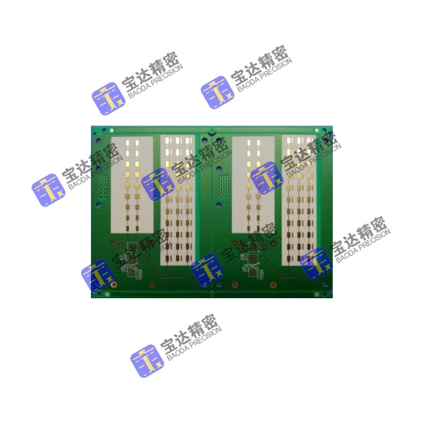
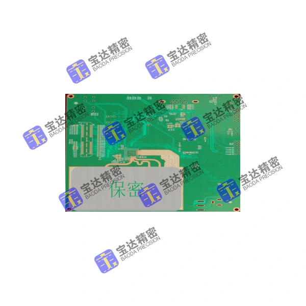
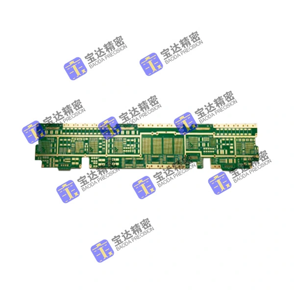
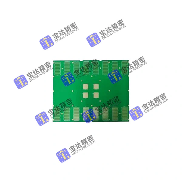
Start with the test interface, copper stack or RF laminate.
Guangde Baoda Precision Circuit · 广德宝达精密电路有限公司 describes an operation established in September 2012 in the Guangde PCB Industrial Park, Anhui. Its introduction focuses on medium and small lots, high-layer-count boards, heavy copper and mixed-material constructions.
The catalogue is particularly useful for semiconductor-test interfaces and thick power boards: it gives board thicknesses, named blind-via sequences, local gold treatments and large outlines. Those details make a better starting brief than selecting only the highest layer count.
Sixteen separate examples appear below, each with its corresponding original image. Their numerical facts stay with that construction. General drilling minima, trial-development milestones and RF application labels do not become universal production guarantees.
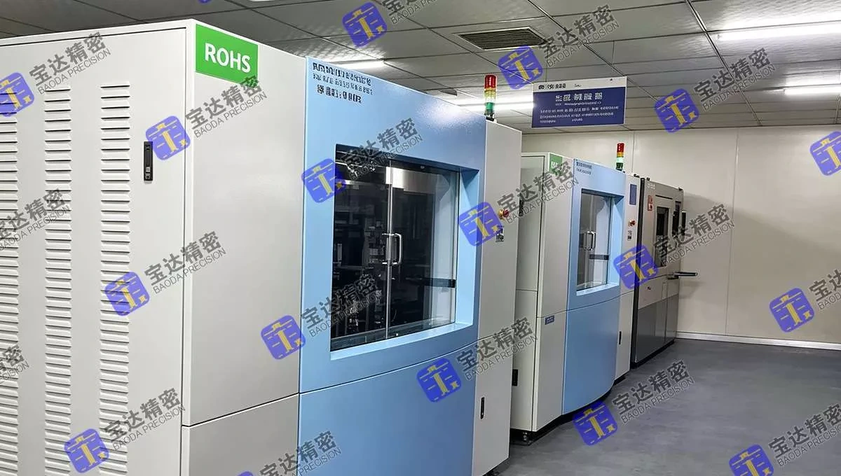
Vacuum lamination press — original manufacturer equipment gallery. A process photograph is not a released stack or reserved capacity.
Company milestones are development records, not one capability ceiling
The introduction describes 60 mu, a first-phase investment of RMB 150 million, a 10,000 m² workshop and designed annual capacity of 300,000 m². These describe the project as presented, not current available production slots.
The timeline separates a 42-layer backplane trial in 2016, large chip-test volume constructions in 2020–2021, and a 26-layer, 13 mm thick lithography-equipment board in development in 2022. Its 2025 seven-step backdrill milestone gives 4 mil from backdrilled hole to line, which is not a minimum line/space pair. A 2026 airtightness breakthrough has no stated leak-test pressure or acceptance result. Ask for the released construction, maturity, lot quantity and current schedule for your design.
SEMICONDUCTOR TEST / MECHANICAL AND CONTACT DATUMS
A chip-test board is an interface, not just a layer count.
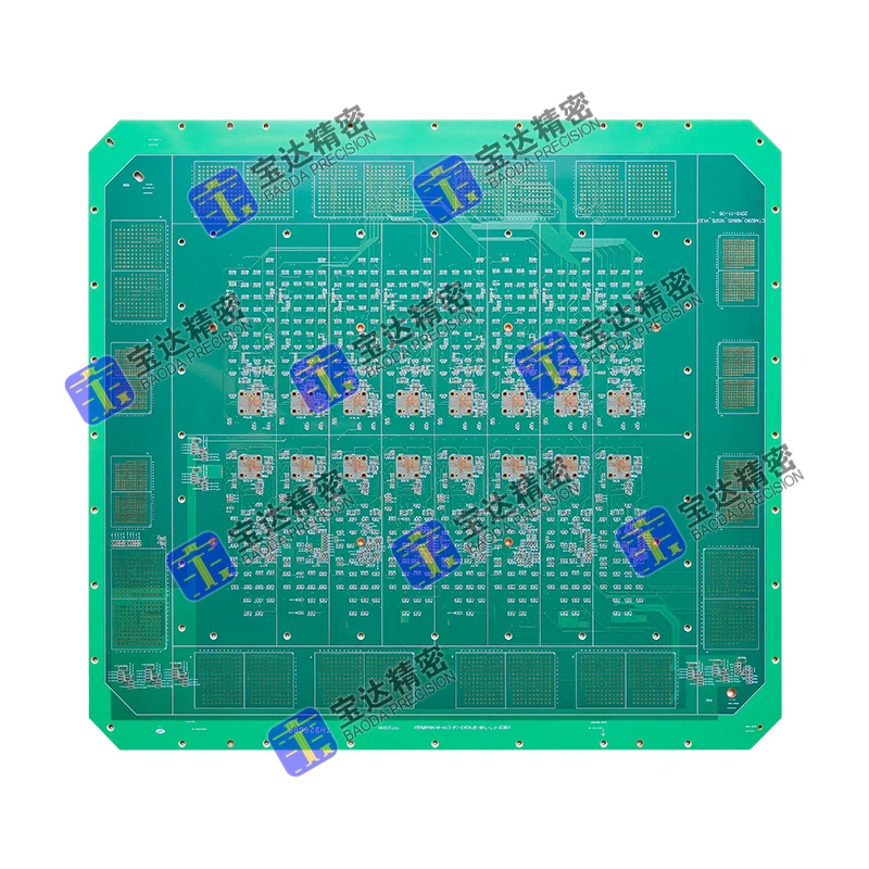
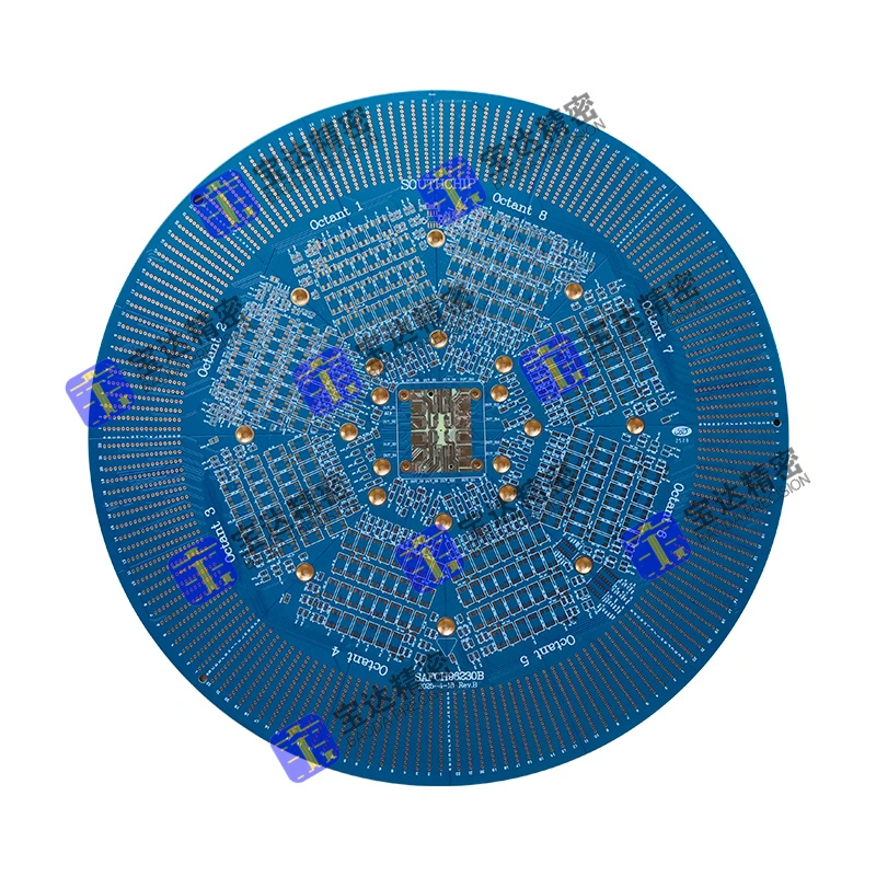
Large outlines and thick stacks put probe alignment, flatness, contact metallurgy and via depth into the RFQ. The source names several quite different test constructions; a 658 × 588 mm board, a stepped blind slot and local hard gold should not be collapsed into one generic “high-layer PCB” entry.
Corresponding original Baoda catalogue photograph
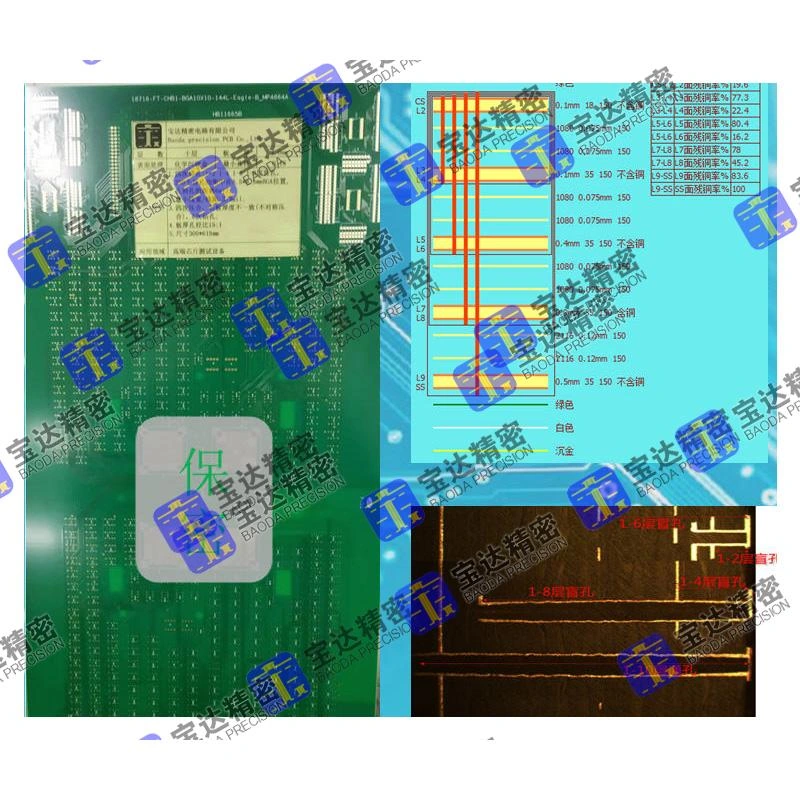
12-layer large-format chip-test PCB
Outline
658 × 588 mm
Thickness
5 mm
Via route
Blind holes; 0.4 mm minimum hole label
Finish
Chemical nickel/gold
Release probe/contact geometry, flatness and mechanical datums across the 658 × 588 mm board. Define the blind-hole depth, finish specification and finished-hole tolerances.
Corresponding original Baoda catalogue photograph
18-layer stepped blind-slot chip-test PCB
Thickness
6.35 mm
Hole label
0.20 mm
Aspect-ratio title
31.7:1
Route
Stepped blind slot
Finish
Immersion gold
Release the stepped-slot depth, registration and interface datums, not only total board thickness. Confirm TG170 material grade, plating acceptance and the aspect-ratio basis.
Corresponding original Baoda catalogue photograph
26-layer, two-step blind-via chip-test PCB
Thickness
6 mm
Via route
Two-step blind vias
Hole label
0.15 mm; finished status unspecified
Finish
Electroplated nickel/gold plus local thick gold
Aspect-ratio title
30:1; hole/thickness basis needs clarification
Do not derive an approved aspect ratio by dividing overall board thickness by the smallest hole label. Ask which hole depth and diameter support the 30:1 title, and define local gold zones and thickness.
Corresponding original Baoda catalogue photograph
32-layer chip-test PCB with local hard gold
Thickness
6 mm
Aspect-ratio title
30:1
Hole label
0.20 mm
Source gold wording
Whole-board 3u plus local hard gold 20u; unit undefined
Define the gold unit, measurement method and hard-gold/contact zones. The source writes u without defining it; it is not converted to micrometres or microinches.
Specify a hole depth, not a ratio computed from unrelated rows
The 26-layer title says 30:1, while its details give 6 mm overall thickness and a 0.15 mm minimum hole label. The source does not explain whether that minimum is through, blind or finished. Do not turn overall thickness divided by the smallest label into a qualified through-hole ratio. Supply the individual hole depths and acceptance microsections.
The 32-layer page writes gold values as 3u and 20u without defining the unit. State microinches or micrometres explicitly, identify local hard-gold zones and agree how thickness is measured.
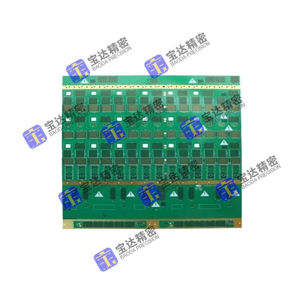
Corresponding original Baoda catalogue photograph
10-layer, four-step blind-via chip-test PCB
Thickness
3 mm
Build-up
Four-step blind vias
Hole label
0.20 mm
Finish
Immersion gold
Provide the four-step via map, lamination sequence, pad registration and test-interface tolerances. The company history also mentions a different five-step construction; it is not assigned to this product.
Corresponding original Baoda catalogue photograph
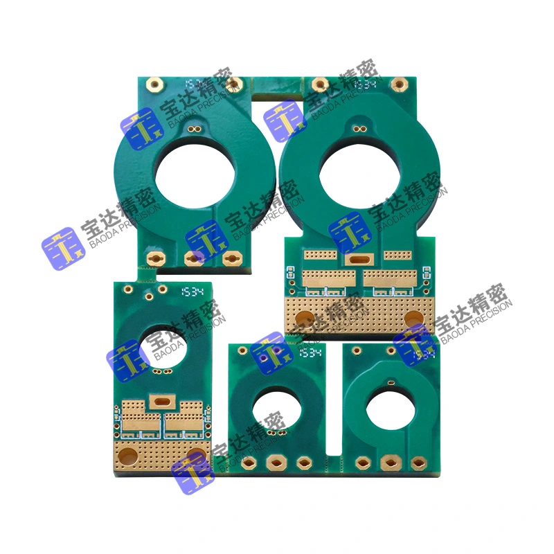
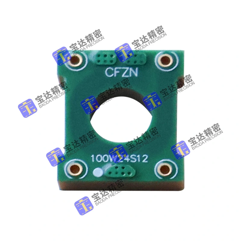
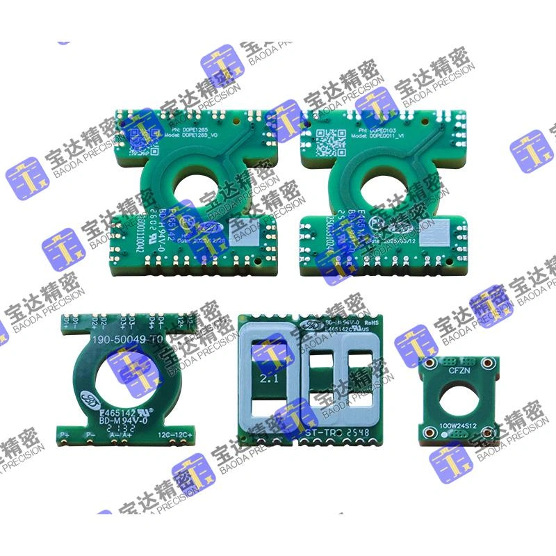
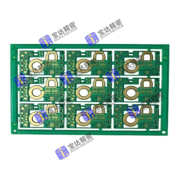
42-layer station-board catalogue example
Source title
工作基站板
Thickness
5 mm
Hole label
0.50 mm
Finish
Immersion gold
Confirm the actual station function and released stack. The source title is retained without assuming a mobile-network standard, link speed or production-volume approval.
LITHOGRAPHY-EQUIPMENT POWER & COILS / COPPER BY LAYER
Separate total thickness, finished copper and winding performance.
Baoda's two lithography-equipment power boards have unusually thick headline constructions. “Lithography equipment” describes the customer's board application; it is not a claim that the PCB factory makes semiconductor lithography machinery.
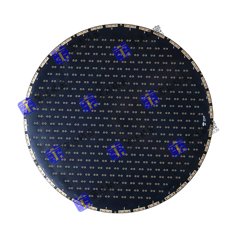
Corresponding original Baoda catalogue photograph
22-layer lithography-equipment power PCB
Copper
4 oz finished copper; title total copper 3 mm
Thickness conflict
Title 13.5 mm; detail row 8 mm
Hole label
2.7 mm; finished status unspecified
Finish
Immersion gold
Resolve the 13.5 mm title versus 8 mm detail before quoting. Release the thickness datum, layer-by-layer finished copper, current/temperature limits and the actual finished-hole drawing.
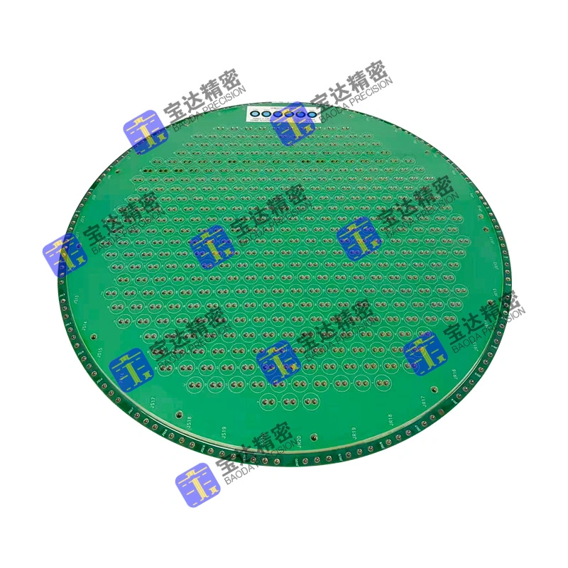
Corresponding original Baoda catalogue photograph
30-layer lithography-equipment power PCB
Copper
4 oz inner and outer
Total copper title
4.2 mm
Total thickness title
13.5 mm
Confirm the relationship between individual copper weights, total copper and overall thickness. Specify press construction, connector/slot tolerances and acceptance microsections; do not combine this title with the generic chart.
Three coil constructions with different release requirements
The 18-layer resin-filled design, 12-layer 6 oz transformer design and 12-layer two-step blind/buried design are separate catalogue examples. “Inductance and resistance control” supplies no target value, test frequency or tolerance.
Corresponding original Baoda catalogue photograph
18-layer resin-filled blind-via coil PCB
Copper
4 oz inner and outer
Thickness
3 mm
Hole label
0.30 mm
Route
Resin fill and blind vias
Finish
Immersion gold
The source material field describes resin filling and blind vias, not a laminate grade. Specify dielectric, conductor resistance, fill/cap requirements and the coil test conditions.
Corresponding original Baoda catalogue photograph
12-layer, 6 oz coil PCB
Copper
6 oz finished, inner and outer
Thickness
3.5 mm
Via route
Buried holes
Finish
Immersion gold
Application
Transformer
Release finished copper and dielectric on every layer, winding connections, conductor resistance and isolation requirements. No numerical inductance or current rating is supplied.
Corresponding original Baoda catalogue photograph
12-layer blind/buried-via coil PCB
Build-up
Two-step blind/buried vias
Electrical wording
Inductance and resistance control; no numerical target
Specify inductance and resistance values, tolerances, temperature/frequency and test fixtures. Material, thickness, holes and finish are not stated for this separate coil example.
Corresponding original Baoda catalogue photograph
18-layer FR-4 heavy-copper PCB
Copper
4 oz inner and outer
Thickness
3 mm
Hole label
0.30 mm
Finish
Immersion gold
Specify each layer copper and dielectric, conductor spacing, plating and thermal rise. This catalogue example supplies no universal power rating or minimum line/space.
A named laminate still needs a layer assignment and test plan.
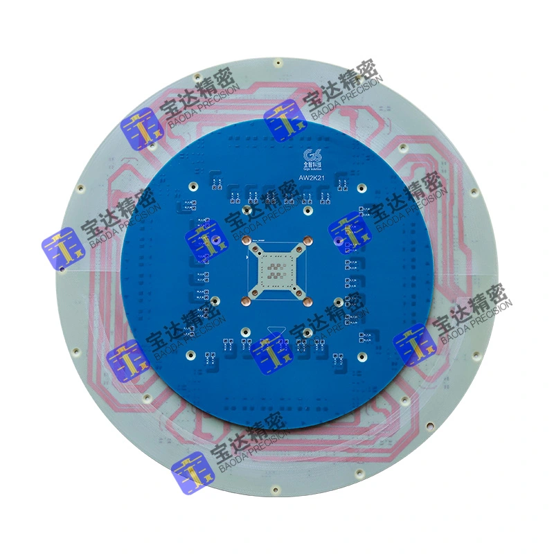
Two six-layer examples name Rogers materials mixed with FR-4. The 14-layer example names Panasonic M6 and RA300A, adds embedded resistance and a wrapped metal edge, and combines blind vias with backdrilling. Keep the laminate, via construction and measured signal requirements tied to the actual stack.
Corresponding original Baoda catalogue photograph
6-layer RO4350B / FR-4 hybrid RF PCB
Thickness
1.2 mm
Build-up
Two-step blind vias
Hole label
0.20 mm
Finish
Immersion gold
Source application
24G radar
Define RO4350B layer positions, bond materials, copper profile and RF coupon results. The 24G application label is not a measured insertion-loss result.
Corresponding original Baoda catalogue photograph
6-layer RO3003 / FR-4 hybrid RF PCB
Thickness
1.0 mm
Build-up
Two-step blind vias
Hole label
0.20 mm
Finish
Immersion gold
Source application
77G radar
Release the exact RO3003 grade, FR-4 and bond layers, copper profile, impedance geometry and test frequency. The 77G label does not establish a loss budget or delivered RF performance.
Assign both materials to the approved stack and define resistor value/tolerance and processing. Specify edge-wrap coverage, backdrill layers and RF/high-speed acceptance; no numerical resistor or impedance tolerance is published.
Corresponding original Baoda catalogue photograph
20-layer, seven-step backdrilled high-speed PCB
Thickness
4 mm
Material
Panasonic M6 R5775(G)
Route
Seven-step backdrilling; impedance control
Hole label / finish
0.20 mm / immersion gold
Application
Chip testing
Provide a layer-specific backdrill table, residual-stub limits and impedance coupon geometry. The source supplies no numerical impedance tolerance, so that filter stays unknown.
Put the RF and backdrill deliverables in the order
Supply design frequency, controlled-line geometry, laminate/bond grade by layer, copper profile, impedance target and tolerance, coupon and measurement reference. For backdrilling, identify start/stop layers, diameter, depth datum, residual-stub limit, adjacent-copper clearance and reporting.
The catalogue's 24G and 77G radar descriptions are application labels. No measured insertion loss, numerical impedance tolerance, resistor tolerance or backdrill residual-stub result is published for these examples.
GENERAL PROCESS CHART / STANDARD, ADVANCED AND ENGINEERING
The engineering column is a discussion scope, not the default quote.
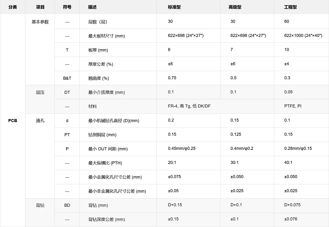
The official image chart uses three named columns. It does not state that all rows can be delivered together. Its 60-layer engineering row also has a different basis from the 42-layer trial history and the individual product catalogue.
Standard
Layers / thickness
30 / 6 mm
Maximum panel
622 × 698 mm
Minimum mechanical drill
0.20 mm
PTH aspect ratio
20:1
Thickness tolerance / bow-twist
±8% / 0.75%
Advanced
Layers / thickness
30 / 7 mm
Maximum panel
622 × 698 mm
Minimum mechanical drill
0.15 mm
PTH aspect ratio
30:1
Thickness tolerance / bow-twist
±6% / 0.5%
Engineering
Layers / thickness
60 / 10 mm
Maximum panel
622 × 1000 mm
Minimum mechanical drill
0.10 mm
PTH aspect ratio
40:1
Thickness tolerance / bow-twist
±4% / 0.3%
The chart gives minimum dielectric 0.10 / 0.10 / 0.05 mm, PTH dimensional tolerance ±0.075 / ±0.050 / ±0.050 mm and NPTH tolerance ±0.050 / ±0.025 / ±0.025 mm. Backdrill diameter is expressed as D + 0.15 / D + 0.10 / D + 0.075 mm, with depth tolerance ±0.15 / ±0.10 / ±0.076 mm. Clarify D and the actual stack before applying these figures. Mechanical drill diameter is not a finished plated-hole minimum.
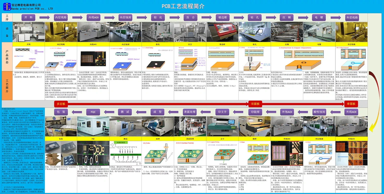
Original capability image and production flowOriginal table retains its source column definitions.Published flow connects inner-layer imaging/AOI, lamination, drilling/plating, outer layers, mask, finish, profiling, test, FQC and packing. Agree actual process responsibility for your order.
EQUIPMENT TO SHIPMENT / ASK FOR LOT-LINKED OUTPUT
Equipment supports the conversation. Reports release the lot.
CCD alignment / backdrilling
Hole, fill and registration evidence
The gallery names CCD backdrilling, X-ray target drilling, CNC drilling, vacuum lamination, vacuum resin filling, LDI and AOI. Ask for the actual blind/buried sequence, fill/cap specification, registration and microsections. Instrument-level resolution and line descriptions are not automatically transferred to the product filter.
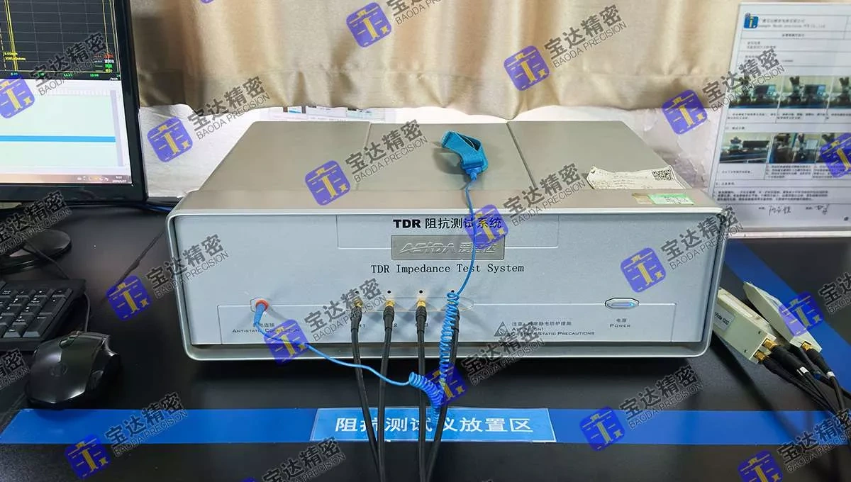
TDR impedance testing
Signal requirements and material lots
Agree target, tolerance, geometry, layer, coupon and report. Link mixed-laminate and embedded-resistor builds to material lot records and the approved engineering revision. A TDR photograph establishes an item in the published equipment gallery, not the result for your board.
Four-wire, eight-axis flying-probe testing
Coil resistance, continuity and shipment evidence
The test gallery also lists four-wire fixture testing, coating thickness, ionic contamination, reflow, peel strength, metallography and hole-copper measurement. Select resistance/isolation thresholds, sampling, finish and dimensional evidence appropriate to the construction. Ask how reports identify the actual lot and data revision.
GUANGDE SITE / DATED DOCUMENTS AND RESPONSIBILITY
Match documents to the entity and the work being quoted.
The qualification copies name Guangde Baoda Precision Circuit Co., Ltd., credit code 91341822054451157M, and operation address No. 9, First Guihua Road, PCB Industrial Park, Guangde Development Zone. A registered-address description uses the boundary between Beihuan, Jingtang and First Guihua roads. Keep supplying-site, process and contractual responsibility explicit.
IATF and environmental management copies: scope and dates
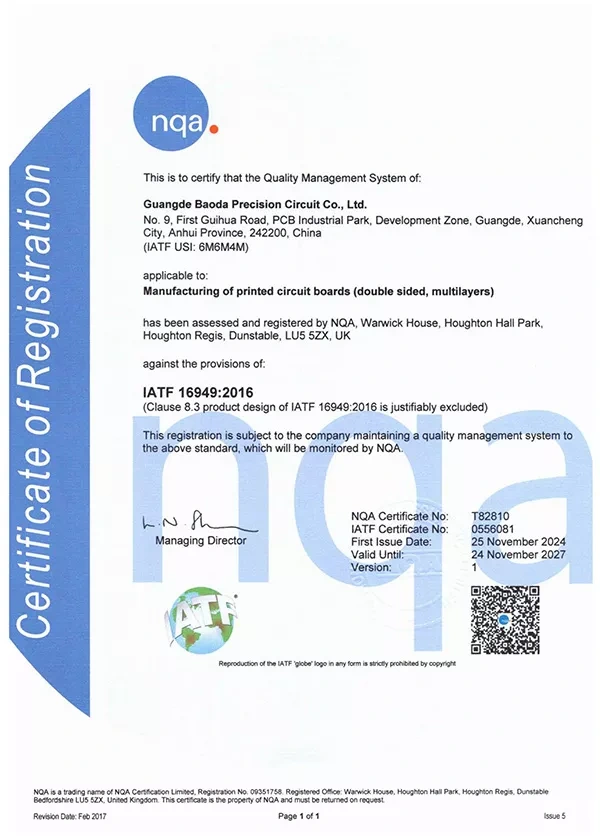
The NQA IATF 16949:2016 copy gives T82810 / IATF 0556081, site USI 6M6M4M, first issue 25 November 2024 and validity to 24 November 2027. Scope is manufacturing double-sided and multilayer printed circuit boards, excluding product design under clause 8.3.
The ISO 14001:2015 copy E5533 is reissued 9 September 2024 and valid to 14 September 2027, covering production and sales of single-sided, double-sided and multilayer PCBs. These are manufacturer-hosted copies; current issuer surveillance/register standing was not independently established. The introduction also claims ISO 9001 and UL, but no current UL ownership badge is inferred from that sentence.
IATF copy: use the stated entity, scope and validity.Environmental management copy; not an emissions result.
Operating permit and October 2026 occupational-health record
The Guangde government Q2 permit list, published 9 July 2026, names Baoda under permit 91341822054451157M001V, simplified management, validity 18 November 2022 to 17 November 2027, with an adjustment processed 2 April 2026. Its rectification-needed field says “否” for that list entry. This does not establish continuous compliance in every regulatory area.
A separate occupational-health inspection notice published 8 October 2026 records five findings for the same entity: principal/health-manager training, the management organisation/system, required worker health rechecks, worker hazard notification and current occupational-hazard assessment. The results field reads “无”; the reviewed notice does not show closure or confirm rectification.
Ask for the current occupational-health follow-up and closure evidence in supplier qualification. These are dated workplace findings, not evidence of PCB electrical defects, and neither are they erased by the permit-list wording.
A tenant project is not Baoda's own available capacity
The government's July 2026 investment-filing list, published 6 August 2026, identifies 广德先胜电子科技有限公司 as a separate entity planning to lease approximately 6,000 m² from Baoda at No. 9 First Guihua Road. The filing describes planned plating/finish and lamination toll-processing capacity.
The filing is not proof of operation, Baoda-owned production capacity or a statement that your order is outsourced. Ask which entity and line perform each quoted process, what the current site arrangement is, and who provides lot and regulatory records.
SOURCE TRAIL
Sources behind this profile
Individually researched 9 October 2026. Sixteen corresponding original product pages/photos, company history and contacts, process charts, production/test galleries, original qualification copies and three complete government records. Source discrepancies remain visible. General engineering limits, certificate copies and dated regulatory records retain their own scope; they do not approve a combined construction or establish current issuer standing.