Start with the battery interface, then choose the board construction.
Assunny’s catalogue concentrates on battery-protection boards, flexible circuits and assembled collection interfaces. Its company page describes an origin in Shenzhen in 1996, an earlier Bao’an manufacturing base and a current manufacturing base in Jiujiang, Jiangxi. The same website now names 江西爱升精密电路科技有限公司 and lists a Shenzhen sales centre. This retained directory entry represents 深圳市爱升精密电路科技有限公司; the current brand website supplies the manufacturing information below. Confirm the contracting entity and producing site together.
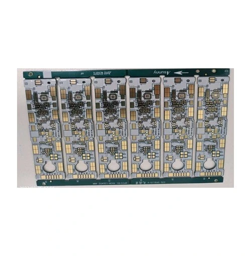
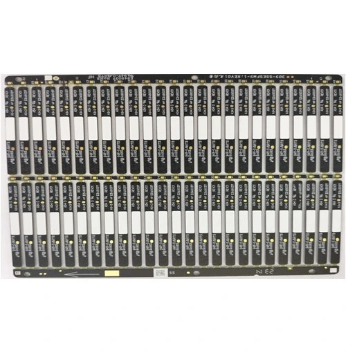
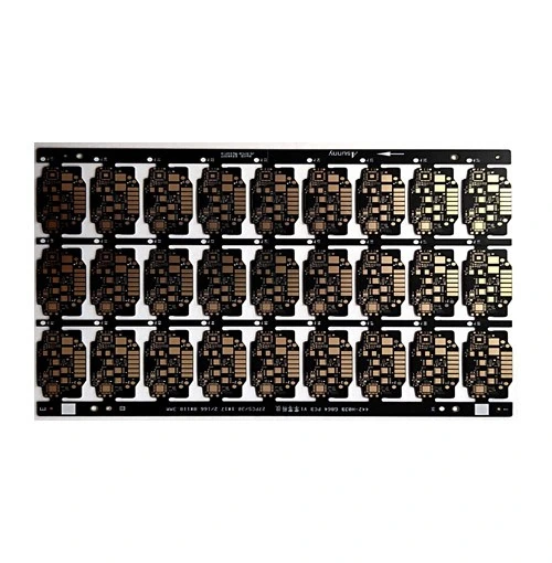
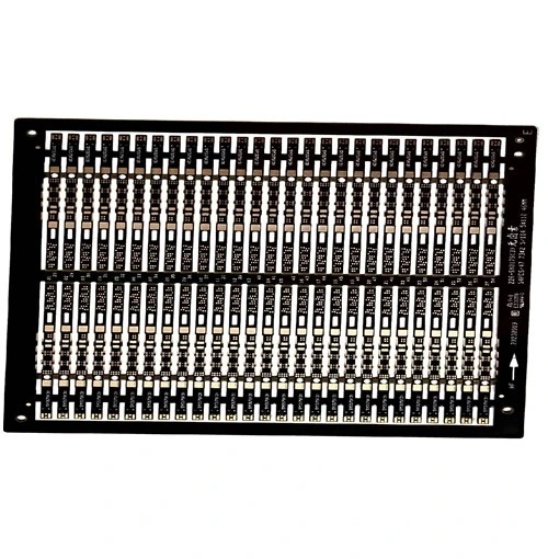
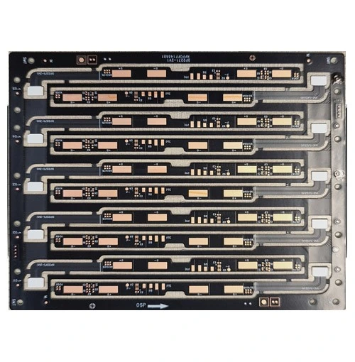
The first three photographs come from the manufacturer’s battery-protection PCB page. Their four-layer labels do not make them the same process. No board thickness, finished-hole diameter, current rating or trace minimum is published alongside these particular entries.
Ask which side carries the aluminium base, how copper layers are insulated from it and which drawing defines the thermal interface. Release mounting datums and metal clearances. Agree the dielectric, insulation test and thermal acceptance for the actual assembly; the catalogue label alone gives no thermal-resistance value.
Four-layer through-hole PCB with steel plate; phone battery application.
Steel-plate battery interface
Define the steel grade, thickness, attachment method and keep-out zones. Ask how flatness and attachment are inspected after assembly. Clarify whether the steel is a mechanical support or another designed interface; it should not inherit the aluminium example’s thermal assumptions.
Four-layer through-hole, copper-paste filling and capped plating; drone battery application.
Copper-paste filled & capped
Specify the holes requiring fill, cap thickness and allowed voids or surface depression. Ask for the fill material, process sequence and agreed microsection evidence. Copper paste is not automatically solid plated copper fill, and neither a drone label nor a board photograph establishes a current-carrying rating.
TWO SIX-LAYER EXAMPLES / DIFFERENT TERMINATIONS
Keep the flex transition and the metallised edge on the drawing.
Show the metallised edge by datum, extent and continuity requirement. Release the finish zone, edge-to-copper features and the inspection method. Separately define the flexible section, coverlay, stiffener and installation bend. This six-layer construction has no published edge-plating thickness or bend-life result.
Six-layer rigid-flex; tablet battery application.
Rigid-to-flex battery connection
Define how many of the six layers continue through the flex zone; the source gives total layers only. Send the installed geometry, connector engagement and whether movement is static or repeated. Ask for the proposed copper, adhesive and coverlay construction before accepting a bend radius. The edge-metallisation feature in the neighbouring example does not apply here by default.
The FPC application page also shows six-layer rigid-flex for smartwatch and phone batteries and lists automotive collection harnesses, camera modules and wearable applications. These are application routes, not evidence that every photographed circuit carries the same layer stack or bending requirement.
PROCESS TABLES / COMPARE LIKE WITH LIKE
Read PCB sample limits separately from the dated FPC production table.
PCB · volume / sample
Layer range
1–14 / 1–18
Inner and outer line / space
0.07 / 0.07 mm volume; 0.05 / 0.05 mm sample
Finished inner copper
12–105 µm / 12–210 µm
Finished outer copper
12–105 µm / 12–140 µm
Plating aspect ratio
10:1 / 12:1
Minimum mechanical drill bit
0.15 mm volume; sample not stated
The volume thickness range is 0.2–3.2 mm. The materials row names FR-4, high-frequency/high-speed, aluminium-base and embedded-copper constructions; PTFE appears additionally in the sample column. It gives no laminate brands or approved substitutions for these catalogue boards.
FPC · 2024 volume / small batch
FPC layer range
2–8 / 2–16
Rigid-flex layer range
2–16 / 2–20
Panel size
500 × 1,200 / 500 × 1,500 mm
Inner line / space minimum
0.030 / 0.025 mm
Rigid-flex thickness minimum
0.30 / 0.25 mm
Laser-hole / ring notation
0.05 / 0.19 mm volume; 0.05 / 0.15 mm small batch
This chart has 2022, 2023 and 2024 columns. The figures here are specifically from 2024; “small batch” is not the PCB table’s sample column. Request an updated process window and the proposed rigid/flex stack for the order.
Three details to resolve in engineering review
Hole definitions: the PCB table distinguishes a mechanical drill bit and a laser hole. Neither is a confirmed finished plated-hole diameter for one of the photographed products.
Impedance condition: one PCB row labelled differential/characteristic >50 Ω gives ±10% volume and ±8% sample. A second row also says characteristic >50 Ω but gives ±10 ohm for volume. Ask which condition applies; do not turn both into one tolerance.
FPC transcription: a base-copper heading is followed by hole/ring-like values, while another laser-hole heading contains micrometre copper-like ranges. Those ambiguous rows are omitted rather than silently relabelled. The 2024 finish entry also spells “NIG”; obtain the intended finish specification.
These general tables do not establish one achievable combination of maximum layers, minimum routing, metal base, fill and impedance. Select the actual construction and request a returned stack, process route and acceptance limits.
ASSEMBLY HANDOFF / BATTERY COLLECTION INTERFACE
A collection assembly needs more than a bare-board capability chart.
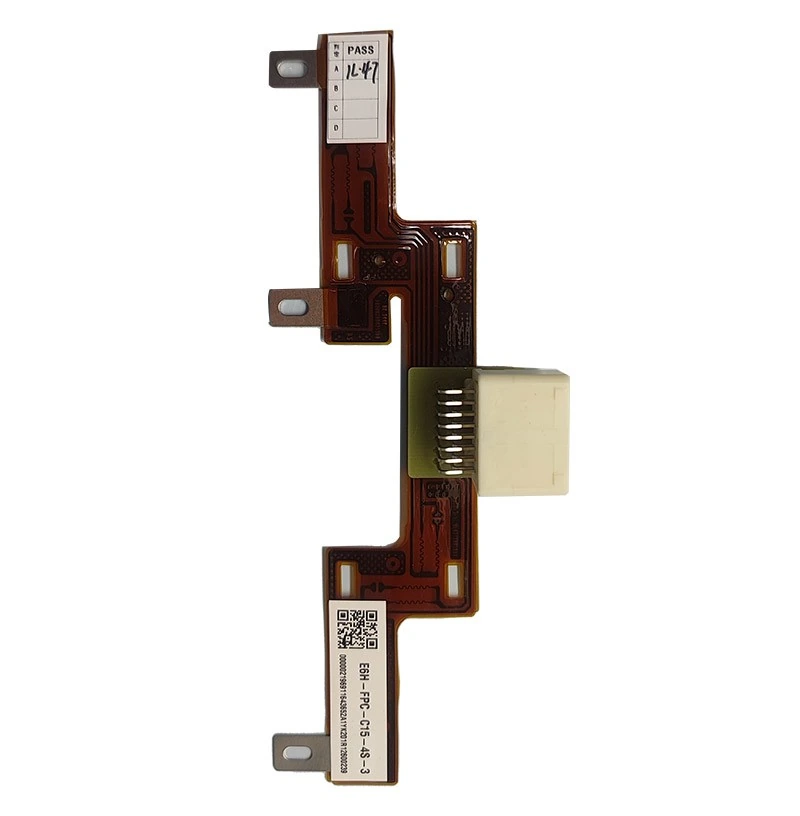
Connector-overmoulded FPCA, shown in the manufacturer’s power-battery SMT catalogue.
Connector-overmoulded FPCA
The same catalogue shows single-row through-pin and cutout-board designs as distinct alternatives. For the overmoulded connector route, identify the exact connector, termination method, pin map, encapsulation boundaries and accessible test points. Release insulation, continuity and mechanical acceptance for the delivered assembly. No pin count, voltage, waterproof rating or pull-force result is inferred from the photo.
The SMT process table lists board processing from 50 × 50 to 1,200 × 370 mm, board thickness 0.3–6 mm, and BGA/CSP minimum ball pitch 0.30 mm with 0.15 mm ball diameter. It separately lists printing up to 2,000 × 450 mm. A printing envelope does not prove placement over the same envelope; obtain the actual panel transport and fixture plan.
Before assembly
Supply the BOM, approved alternates, placement data, connector drawings and flexible-section handling instructions. Define who approves substitutions and who supplies components.
At acceptance
Agree the pin-map test, insulation conditions, fixture, sampling and lot traceability. For a battery collection interface, confirm the delivered circuit scope and system responsibility rather than assuming a complete battery-management system.
The equipment galleries name FPC AOI, roll-to-roll coverlay and lamination, Schmoll drilling, laser processing, automatic testing and thermal shock, and PCB inspection and plating equipment. These manufacturer-labelled listings explain process coverage; they are not machine calibration records or proof of an assigned production line for this order.
CURRENT MANUFACTURING LOCATION / CONTRACT SCOPE
Qualify the Jiujiang plant and the entity on the quotation.
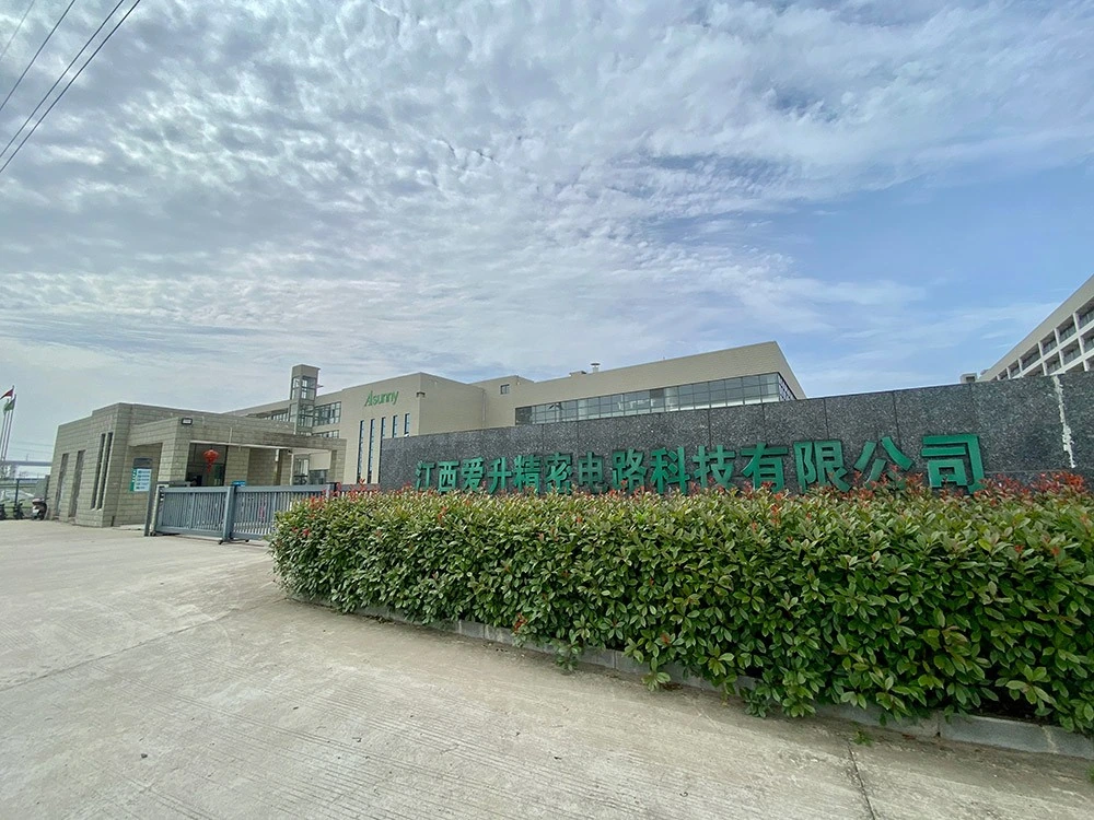
Original photograph labelled 江西工厂外观 — Jiangxi factory exterior. Publication is not a site audit.
Current website locations
Jiujiang headquarters: 128 Gangxing Road, Chengxi Port Area, Jiujiang Economic and Technological Development Zone, Jiangxi.
Shenzhen sales centre: Unit 2603, Qianhai Chow Tai Fook Financial Building, 66 Shuniu Street, Nanshan, Shenzhen.
On 15 January 2025, Huangshi’s Economic and Information Technology Bureau reported a visit to 江西爱升精密电路科技有限公司 in Jiujiang concerning voltage-sag management. This independently supports the named Jiangxi business’s activity at that time. It does not certify product quality, establish ownership of the Shenzhen company or validate the current process limits.
The manufacturer’s environmental disclosure index contains documents for both Shenzhen and Jiangxi, including a Jiangxi circuit-board project submission and a 2024 Shenzhen pollution-information spreadsheet. A document index or project submission is not an operating permit or proof that every proposed line is commissioned. Ask for current plant and permit documentation matching the order.
Use the correct certificate holder and production scope.
The company describes ISO 9001, IATF 16949, ISO 14001 and QC 080000 systems, and publishes certificate images. Qualify the holder, address, covered activity, issue/expiry dates and current issuer status. Do not transfer a Shenzhen certificate to Jiujiang, or a bare-board scope to an assembled battery interface. This page does not issue an active certification or UL-ownership badge from those website claims.
The website’s English SGS ISO 14001 image names the Jiangxi entity, certificate CN18/31431, with printed validity from 19 March 2024 to 18 March 2027. The IECQ image gives QC 080000:2017, number IECQ-H SGSCN 24.0016 and the same printed dates. Both describe circuit and assembly activity at 128 Gangxing Road. These are readable manufacturer-hosted documents; continued issuer status and the order’s scope still need confirmation.
For a first enquiry, choose the closest board or assembly above, state the producing site requested and supply the released interface drawing. Ask for the contracting legal name, stack approval, material and finish specification, test plan, production window and delivery records. That answer is more useful than a catalogue-wide maximum layer count.
SOURCE TRAIL
Sources behind this profile
Individually researched 8 October 2026. Original photographs are paired with their own adjoining catalogue labels. PCB sample, PCB volume and dated FPC small-batch columns remain separate. Buyer release guidance is editorial analysis. Current Jiangxi manufacturing information and the retained Shenzhen directory entity are distinguished; no legal-name change or plant audit is inferred.