

MANUFACTURER DOSSIER
Changzhou Aohong Electronics Co., Ltd.
常州澳弘电子股份有限公司 · Changzhou, Jiangsu, China
Company facts at a glance
- Chinese legal name
- 常州澳弘电子股份有限公司
- English name
- Changzhou Aohong Electronics Co., Ltd.
- Short names
- 澳弘电子 · Aohong Electronics
- Listing
- Shanghai Stock Exchange, A-share 605058, listed 21 October 2020
- Founded
- 2005, as 常州澳弘电子有限公司
- Registered address and main plant
- No. 15 Xinke Road, Xinbei District, Changzhou, Jiangsu: double-sided, multilayer and HDI boards
- Other sites
- Changzhou Haihong Electronics (subsidiary), No. 16 Xingtang Road, Changzhou: single-sided boards. Thailand plant: equipment still being installed according to the 2025 annual report. Singapore and Hong Kong companies are sales entities.
- 2025 output and sales
- 4.76 million m² produced and 4.81 million m² sold (2025 annual report). Design capacity is not disclosed; the website’s 7.6 million m² figure carries no date or basis.
- Process capability
- No published process-limit table. Official examples show up to 12 layers, first- and second-order HDI, 0.05 mm line width, and ENIG, immersion tin, OSP, HASL and gold-finger finishes.
- Certificates on the website
- ISO 9001, IATF 16949 (valid to 27 February 2027), AS9100D, ISO 14001; the ISO 45001 and ISO 50001 images show expiry dates that have passed. The certificates seen name the Xinke Road site only.
- UL file
- E303981, printed wiring boards (ZPMV2), holder Changzhou Aohong Electronics Co Ltd
Checked on 29 October 2026 against the 2025 annual report on CNInfo, the official website and UL iQ for Printed Wiring Boards. Certificates are company-published images; confirm current validity with the issuer before relying on them.
Three HDI constructions. Three different release questions.
Changzhou Aohong Electronics Co., Ltd. (常州澳弘电子股份有限公司) publishes double-sided, multilayer and HDI boards from its Changzhou operation. Its HDI catalogue gives individual constructions rather than a single process-limit table. The most useful comparison here is between a power board with plated contacts, a thick-copper automotive board and a fine-line OSP board. Choose the construction closest to your drawing before discussing price or delivery.
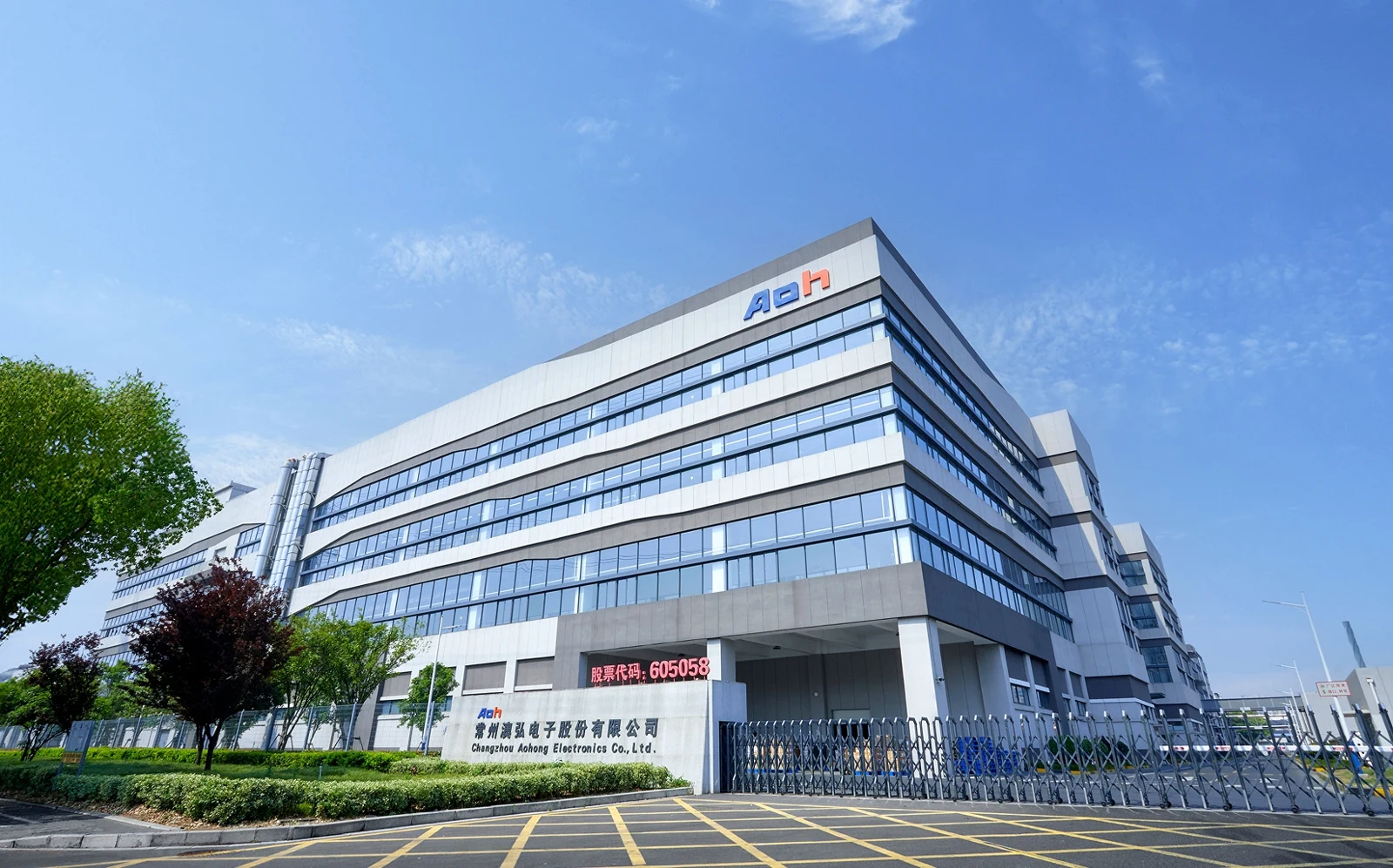
Keep the fabrication entity on the quote.
The contact page assigns double-sided, multilayer and HDI work to Changzhou Aohong at No. 15 Xinke Road, Electronic Industrial Park, Xinbei District, Changzhou. It separately assigns single-sided boards to Changzhou Haihong at No. 16 Xingtang Road. Singapore and Hong Kong entries are offshore business entities; their addresses are not substitutes for the manufacturing address.
The original 2025 annual report confirms the legal English name and describes principally in-house, made-to-order PCB manufacture with a small amount of outsourcing. Its HDI upgrade project had entered volume production. Its Thailand project was still at the equipment installation/commissioning stage in that report. The current contact page lists Thailand across four PCB families; this is a separate site listing, not proof of an approved transfer of your construction.
Specify the contact finish separately from the soldering finish.
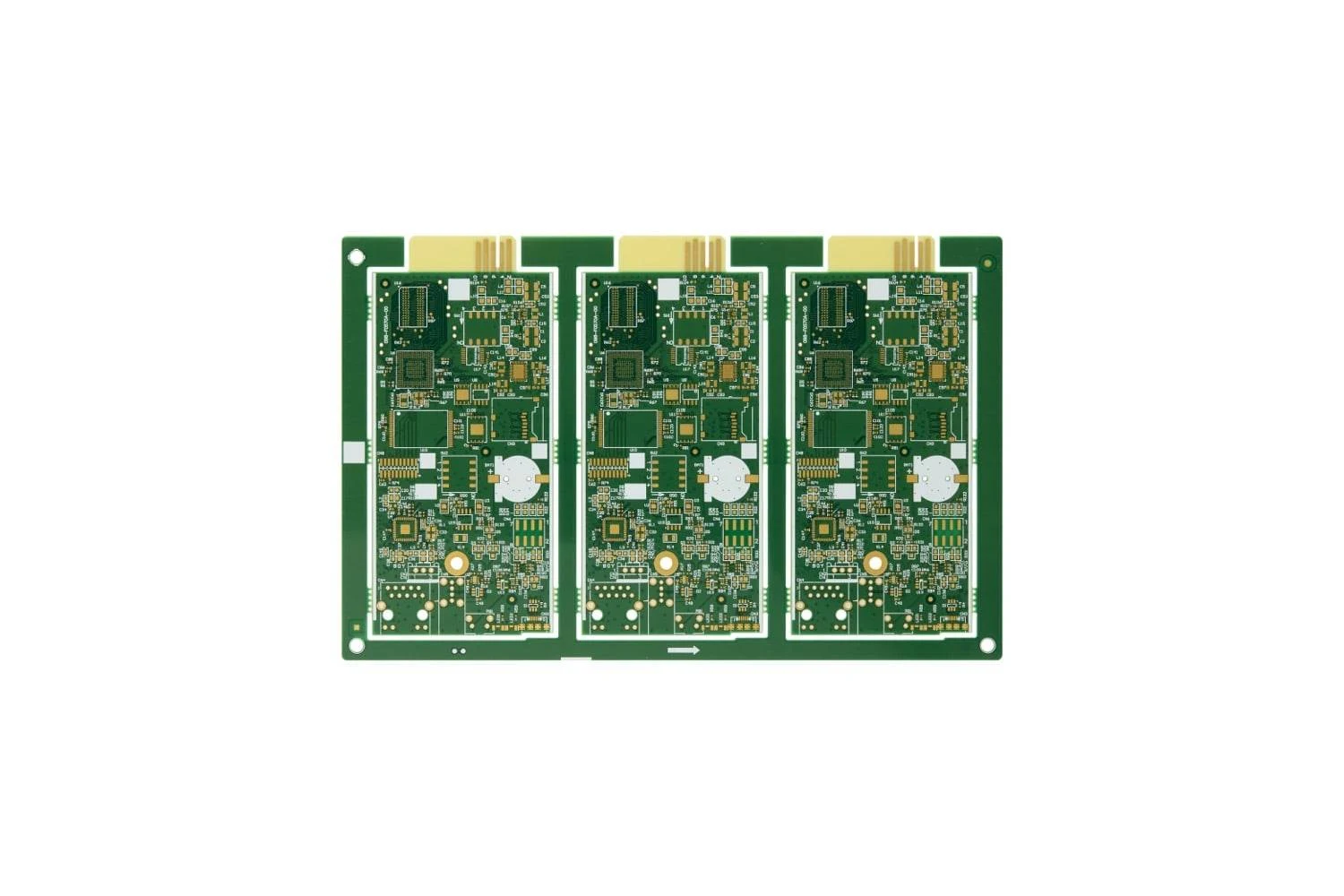
- Construction
- 8 layers · first-order HDI
- Soldering finish
- Immersion gold
- Contact interface
- Plated gold fingers
- Listed application
- Power / energy
The catalogue uses separate wording for the gold fingers and board finish. Define the finish zones on the drawing: which pads are soldered, which contacts mate repeatedly, and which edges need a bevel. Request the proposed contact plating system and thickness, wear requirement, allowable mask encroachment and connector dimensions. “Gold” alone is not a contact-life specification.
For the power circuit, supply finished copper by layer, operating current, thermal boundary conditions and allowable temperature rise. Specify the laminate grade and approved stack. Nothing on this card establishes a copper weight or a current rating; the automotive example below cannot supply those missing values.
Make “thick copper” a layer-specific requirement.
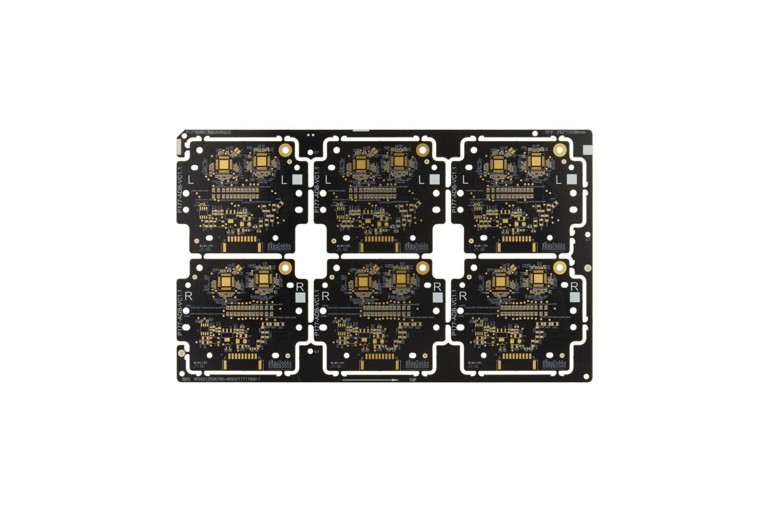
- Board construction
- 6 layers · second-order HDI
- Copper description
- Thick copper; weight unspecified
- Finish / mask
- Immersion gold / black
- Application label
- Automotive electronics
This is a useful starting point when a design mixes power distribution and dense interconnection. Ask for base and finished copper thickness on each layer, the trace/space rule at that copper thickness, and the proposed dielectric after lamination. A thick-copper description does not mean that every layer has the same copper or that a fine signal layer uses the power-plane rule.
Return a via cross-section with the build-up sequence, landing pads, fill/cap requirements and allowed stacked or staggered structures. The second-order HDI label alone does not give microvia diameter, aspect ratio, fill material or acceptable reliability evidence. Agree the thermal-cycle and microsection requirements for the actual stack.
For a vehicle programme, include the applicable customer acceptance, traceability and change-control requirements. An automotive application label does not establish a certificate’s site, current validity or your programme’s approval. The official qualification gallery is a starting point for requesting the relevant current documents.
0.05 mm is the published line width, not a line/space pair.
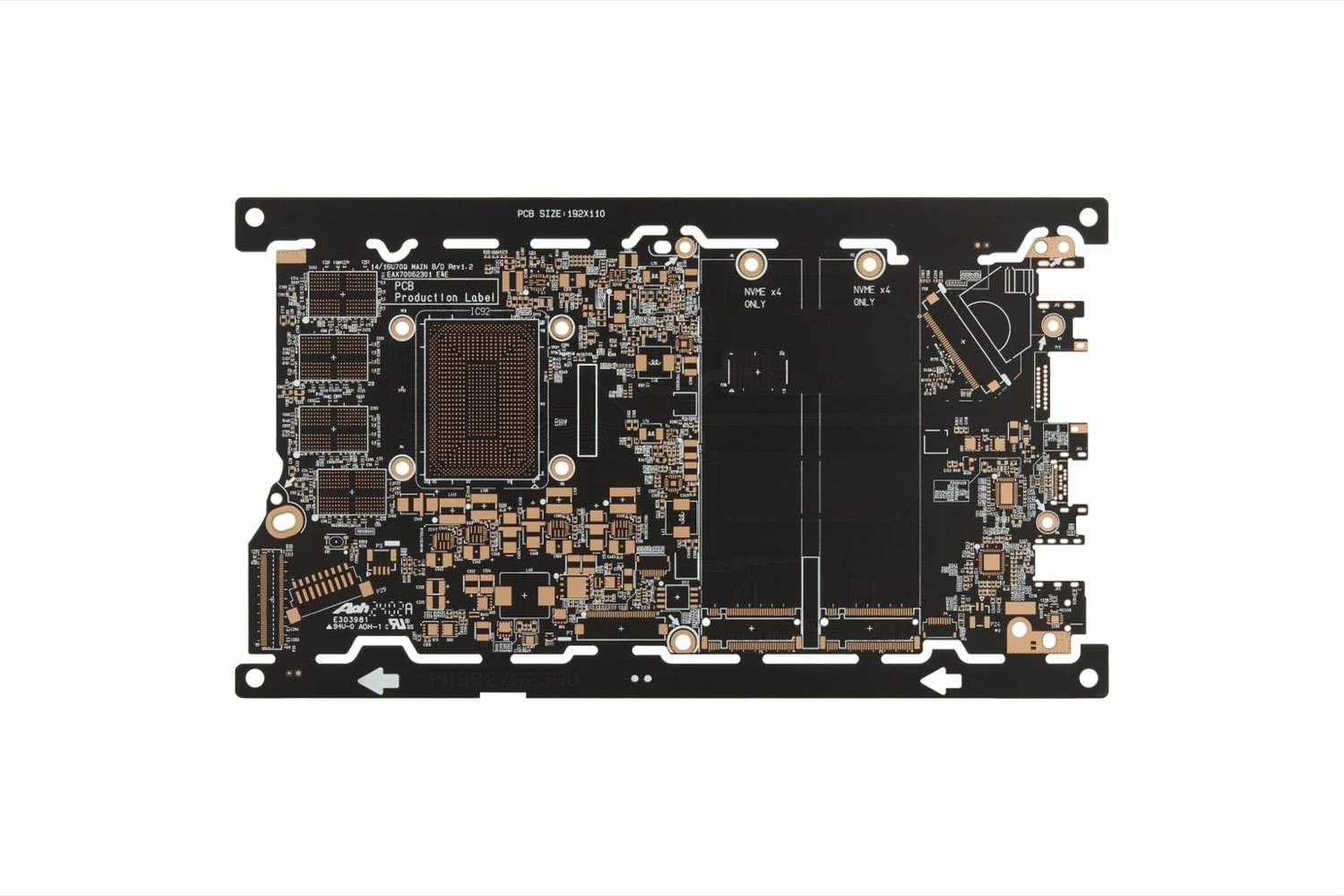
- Construction
- 10 layers · second-order HDI
- Published line width
- 0.05 mm
- Surface finish
- OSP
- Design description
- Multiple BGA / impedance designs
The corresponding card names a line width but no minimum spacing. It mentions impedance designs without a tolerance. Do not turn this into 0.05/0.05 mm routing or assign a ±5% impedance promise. Provide the BGA pitch, escape geometry, paired trace/space by copper layer and target impedance with tolerance.
Request the proposed dielectric, reference planes and coupon definition on the same released stack. If the manufacturer changes copper, glass style or material to accommodate the escape routing, review the resulting impedance geometry before accepting the substitution. A routing value taken from this ten-layer OSP construction does not transfer automatically to the six-layer thick-copper construction.
OSP also needs an assembly handoff. Agree the required finish specification, packaging, storage interval and reflow history with the assembler. The card does not publish a storage life, coating thickness or accepted number of reflows, so those belong in the agreed process plan.
Ask for a proposed construction, not a list of separate extremes.
- Routing & build-up
- Send artwork, netlist, stack, drill map and via structures. Require the returned DFM to identify copper-dependent spacing, sequential lamination, via fill/cap and any changed geometry. Keep power, contact and BGA constraints on one approved revision.
- Line & site assignment
- Name the contracting entity and fabrication site. Ask which HDI imaging, drilling and electrical-test route will handle the order, which operations are outsourced, and what approval is required for a site or process change. The reviewed public pages do not provide a machine-by-machine inventory for these three examples.
- Material & lot release
- Specify approved laminate/prepreg grades, finished copper and finish zones. Agree incoming material traceability, electrical-test revision, microsections, impedance coupons where applicable and first-article acceptance. Brand names, thicknesses and test reports should relate to the quoted construction and shipment lot.
The current official contact page lists gengkf@czaohong.com for this company. Use the PCBVerified shortlist to prepare the selected construction and attach its order-specific requirements. Choose the relevant catalogue example above or use the engineering brief to finish the fabrication pack.
Prepare the engineering RFQ →Sources behind this profile
Individually researched on 8 October 2026. Product photos were matched to the exact official HDI cards and viewed in full; the Changzhou exterior and current logo were checked. Original annual-report pages 5, 12 and 14 were read and visually examined. Company disclosures, product-specific facts and editorial order-review questions are kept distinct. The 2025 project status is dated, not a present-day production guarantee.
- MANUFACTURER / COMPANYCurrent Aohong company description ↗
- MANUFACTURER / SITEChangzhou Aohong, Haihong and overseas contact assignments ↗
- MANUFACTURER / HDIThree illustrated constructions and their exact feature cards ↗
- MANUFACTURER / DOCUMENTSQualification and patent gallery; request current applicable scope ↗
- ISSUER / ORIGINAL REPORT2025 annual report: legal identity, production model and dated projects ↗