

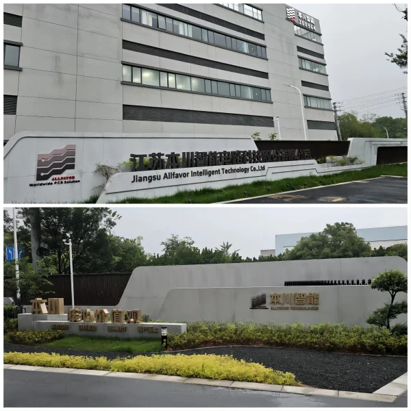
Six layers and 6.0 mm describe different boards.
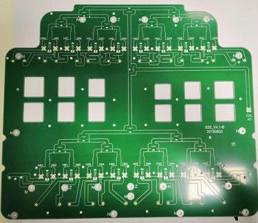
Release the laminate stack.
The source explicitly names six layers and Rogers, but no laminate grade, total thickness, copper weight, RF band or insertion-loss result. Include the exact dielectric family/grade, ply sequence, copper and finish, with impedance geometry and the required coupon or circuit test. A brand name alone does not specify the dielectric properties.
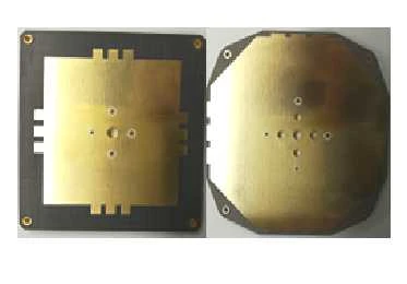
Release the thickness and hole definitions.
The 6.0 mm title belongs to this separate high-frequency entry. Its layer count and laminate grade are not specified. Ask for finished-thickness tolerance, drill and plated-hole dimensions, plating aspect ratio, machining datums and connector interface acceptance. Do not transfer the other board’s six-layer label to this construction.
The RF catalogue also names a Rogers blind-slot board, coupling board and a coverlay-laminated sliding-contact board. For a slot or coupling design, specify depth/datums or the actual coupling geometry and test method; the product names supply no permissible machining tolerance or measured RF performance.
12 oz is a copper label, not a current rating.
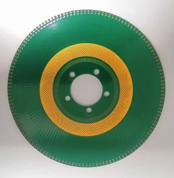
Allfavor labels this example “12OZ厚铜板”. The entry gives no layer count, distribution of copper by layer, base-versus-finished thickness definition, current rating or temperature-rise result. Release the copper schedule and confirm how the quoted thickness is defined and measured.
Specify the conductor spacing, etched geometry and solder-mask requirements at the actual copper weight. Include connection/mounting interfaces and the electrical and thermal acceptance conditions. Ask for cross-section or thickness evidence tied to the order, rather than accepting a generic thick-copper photograph as a thermal qualification.
The published general process table separately lists finished copper up to 6 oz for sample/small orders and 4 oz for large orders. The 12 oz catalogue item therefore needs a construction-specific process agreement; it is not added to those table columns.
Carry the order-size column into the quotation.
The technical page separates sample orders, small lots and large lots. The Chinese and English order-area headings differ at the boundary: the English small-lot column says 2–20 m², while the Chinese label says up to 20 m². State the ordered area and ask which column applies. The compact comparison below keeps the main values in their original columns.
Up to 2 m²
- Layers
- 1–20
- Finished copper
- ½–6 oz
- Plating aspect ratio
- 14:1
- Minimum blind/buried hole
- 0.10 mm
Confirm 2–20 m²
- Layers
- 1–18
- Finished copper
- ½–6 oz
- Plating aspect ratio
- 10:1
- Minimum blind/buried hole
- 0.15 mm
Over 20 m²
- Layer entry
- 12
- Finished copper
- ½–4 oz
- Plating aspect ratio
- 10:1
- Minimum blind/buried hole
- 0.20 mm
Routing depends on base copper.
Before compensation, 35 μm base copper is listed at 3/3 mil line/space for samples and 4/4 mil for both small and large lots. At 70 μm, all three columns list 8/8 mil; at 140 μm, 12/12 mil. The sample column’s finest routing must not be combined with its heaviest copper without an explicit review.
Impedance is not one percentage across all targets.
The source uses ±5 Ω below 50 Ω and ±10% at or above 50 Ω. For example, a 40 Ω target uses the absolute-ohm entry, not an invented ±5% tolerance. Agree the impedance target, stack, measurement method and coupon with the proposed plant.
Company introduction says up to 30 layers, while the 2025 issuer report describes 32 layers as technically achieved. Neither statement replaces the sample/small/large process table. The technical page also contains conflicting millimetre/mil conversions and 1300 versus 1200 mm overlong-board dimensions. Obtain a current drawing-specific confirmation instead of silently resolving those inconsistencies in the factory’s favour.
The table’s minimum drilled aperture is 0.20 mm. That drilling row is not labelled a finished plated-hole minimum. Where finished holes, via fill or blind-hole reliability matter, release those dimensions and acceptance criteria separately.
Link the site to the test record.
The current contact page distinguishes Nanjing/Jiangsu Allfavor, Shenzhen/艾威尔电路(深圳)有限公司, Zhuhai/珠海亚图电子有限公司 and 皖粤光电科技(珠海)有限公司. The 2025 annual report confirms multiple Nanjing, Shenzhen and Zhuhai production bases and identifies the related entities. It describes Thailand as under construction in that reporting period; this is not a claim that a Thai plant is currently available for your order.
The same issuer report describes own production supplemented by outsourced processes or lower-end work when capacity is full. Specify the legal contracting entity, producing plant, outsourced steps, supplier approval and material/lot traceability. Request a change-notification agreement for plant, process or material substitutions.
Agree the RF or copper inspection method.
Official production photographs are labelled LDI exposure, laser cutting, drilling, routing, plasma treatment and automated plating/lamination. Laser cutting is not evidence of laser drilling. Test equipment entries include impedance, intermodulation, gold-thickness and atomic-absorption instruments, but do not provide a complete model, plant assignment or calibration record.
For RF work, specify the impedance or intermodulation test setup, fixture, frequency/power conditions, sample plan and reporting format. For a contact finish, define the measurement method and thickness locations. For thick copper, agree the cross-section and conductor acceptance. A photographed instrument cannot establish that these tests are included in the quoted price.
Make the inquiry construction-specific.
Choose Rogers/RF, thick RF or thick copper; include the material grade, stack, copper schedule, finished/drilled hole definitions, critical geometry, order area and test requirements. Request an annotated process review and named site. The Nanjing factory publishes njsales@allfavorpcb.com; the address was observed on the current official contact page, without a delivery test or marketing message.
Prepare the engineering brief →Sources behind this profile
Individually researched on 8 October 2026. Catalogue examples, technical-table columns and dated issuer statements remain separate. Unresolved source inconsistencies are identified for drawing review rather than converted into guaranteed production limits.
- MANUFACTURER / COMPANYHigh-mix positioning, Nanjing identity and original frontage montage ↗
- MANUFACTURER / SIX LAYERSNamed six-layer Rogers entry and its original photograph ↗
- MANUFACTURER / THICK RFSeparate 6.0 mm high-frequency entry ↗
- MANUFACTURER / THICK COPPERNamed 12 oz board and photograph ↗
- MANUFACTURER / PROCESS TABLESample/small/large lot columns, copper-conditioned routing and target-dependent impedance ↗
- MANUFACTURER / EQUIPMENTProduction labels including LDI and laser cutting ↗
- MANUFACTURER / TESTImpedance, intermodulation and finish-measurement entries ↗
- MANUFACTURER / CONTACTSeparate legal factory names, addresses and Nanjing sales contact ↗
- ISSUER / 2025 ANNUAL REPORTCNInfo p7 entity; p11–13 product/development scope; p13–14 outsourcing; p17 plant projects ↗